
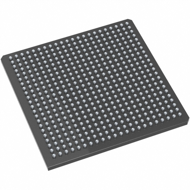
M1A3P600-2FGG144
| Part Description |
ProASIC3 Field Programmable Gate Array (FPGA) IC 97 110592 144-LBGA |
|---|---|
| Quantity | 149 Available (as of June 14, 2026) |

| Product Category | Field Programmable Gate Array (FPGA) |
|---|---|
| Manufacturer | Microchip Technology |
| Manufacturing Status | Active |
| Manufacturer Standard Lead Time | 12 Weeks |
| Datasheet |
Specifications & Environmental
| Device Package | 144-FPBGA (13x13) | Grade | Commercial | Operating Temperature | 0°C – 85°C | ||
|---|---|---|---|---|---|---|---|
| Package / Case | 144-LBGA | Number of I/O | 97 | Voltage | 1.425 V - 1.575 V | ||
| Mounting Method | Surface Mount | RoHS Compliance | ROHS3 Compliant | REACH Compliance | REACH Unaffected | ||
| Moisture Sensitivity Level | 3 (168 Hours) | Number of LABs/CLBs | 13824 | Number of Logic Elements/Cells | 13824 | ||
| Number of Gates | 600000 | ECCN | 3A991D | HTS Code | 8542.39.0001 | ||
| Qualification | N/A | Total RAM Bits | 110592 |
Overview of M1A3P600-2FGG144 – ProASIC3 Field Programmable Gate Array (FPGA) IC 97 I/Os, ~108 Kbits RAM, 144-LBGA
The M1A3P600-2FGG144 is a ProASIC3 family flash FPGA offering 600,000 system gates in a 144-LBGA package. It combines a dense logic fabric of 13,824 logic elements with approximately 108 Kbits of embedded true dual-port SRAM and 97 user I/Os to address mid-range programmable logic requirements.
Designed for applications that require reprogrammable nonvolatile logic, clock conditioning and security features at a single-chip solution, this device targets embedded system designers who need integration, on-chip memory, and flexible I/O in a commercial-temperature FPGA.
Key Features
- Core and Logic 600,000 system gates realized as 13,824 logic elements suitable for mid-density programmable designs.
- Embedded Memory Approximately 108 Kbits of true dual-port SRAM (110,592 total RAM bits) to support buffers, FIFOs and on-chip data storage.
- I/O and Package 97 user I/Os in a 144-LBGA (144-FPBGA, 13×13) surface-mount package for mixed-voltage, banked I/O configurations consistent with ProASIC3 family capabilities.
- Nonvolatile Flash Configuration & Security Flash-based reprogrammable configuration that retains design when powered off and supports secure in-system programming functionality as provided in the ProASIC3 family.
- Clocking and Performance Family-level clock conditioning and integrated PLL resources are available for system clocking and timing control as described in the ProASIC3 documentation.
- Power and Supply Core voltage range specified at 1.425 V to 1.575 V to support low-power core operation; device is surface-mount packaged for standard PCB assembly processes.
- Operating Range and Compliance Commercial-grade operating temperature of 0 °C to 85 °C and RoHS-compliant material status.
Typical Applications
- Embedded control and glue logic — Implement custom control, protocol bridging and peripheral interfacing where mid-range gate density and on-chip SRAM are required.
- Data buffering and packet processing — Use the on-chip true dual-port SRAM for FIFO and buffering functions in communication and data-path subsystems.
- Clocking and timing-sensitive systems — Leverage the family’s clock conditioning/PLL resources for systems that require configurable phase and frequency control.
- Secure configuration and in-system updates — Flash-based, reprogrammable configuration supports design retention and secure in-system programming workflows.
Unique Advantages
- Reprogrammable nonvolatile configuration: Flash-based configuration retains the programmed design when powered off, simplifying field updates and reducing external configuration memory requirements.
- Balanced mid-range resources: The combination of 600k system gates, 13,824 logic elements and ~108 Kbits of SRAM provides a practical balance for many embedded and interface-oriented designs.
- Flexible I/O in a compact package: Ninety-seven user I/Os in a 144-LBGA enable mixed-signal and multi-voltage I/O bank designs without a large package footprint.
- Commercial-grade readiness: Specified for 0 °C to 85 °C operation and RoHS compliance for mainstream commercial applications.
- Low-voltage core operation: Narrow core supply window (1.425 V–1.575 V) aligns with low-power system designs and predictable power budgeting.
Why Choose M1A3P600-2FGG144?
The M1A3P600-2FGG144 positions itself as a practical, flash-configurable FPGA for designers who need mid-density logic, on-chip dual-port SRAM, and a solid set of I/O resources in a compact 144-LBGA package. Its flash-based configuration and family-level security and clocking features support applications that require reliable boot behavior, in-field reprogramming, and integrated timing control.
This device is well suited to engineering teams developing embedded controllers, protocol bridges, and data-path modules that value a reprogrammable single-chip solution with verified logic and memory resources and commercial-temperature operation.
Request a quote or submit an inquiry to receive pricing, availability, and technical purchasing support for the M1A3P600-2FGG144.


Date Founded: 1989
Headquarters: Chandler, Arizona, USA
Employees: 22,000+
Revenue: $8.349 Billion
Certifications and Memberships: ISO9001:2015, IATF16949:2016, AS 9100D


