
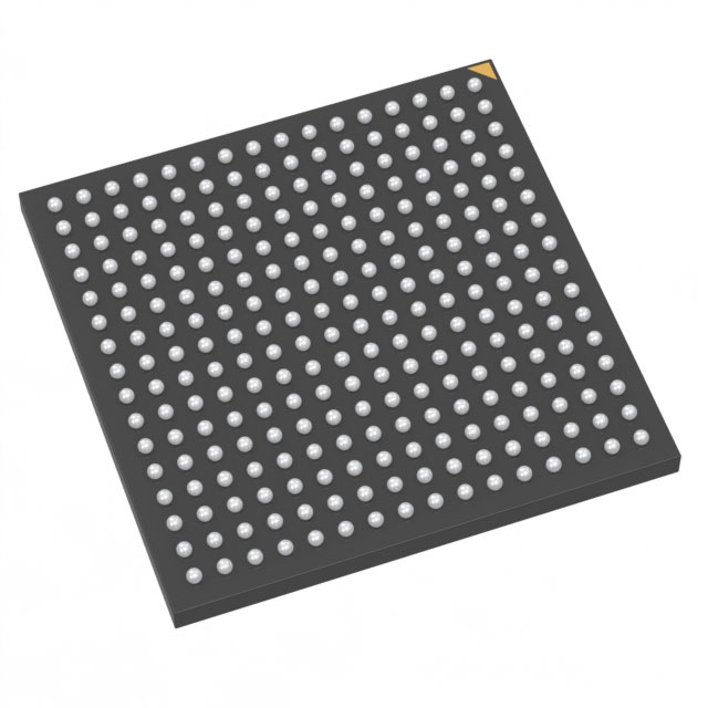
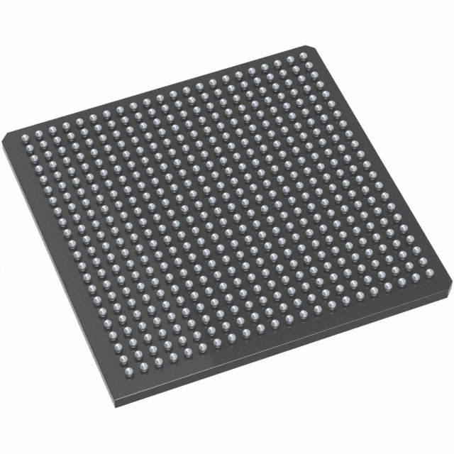
M1AFS1500-FG676
| Part Description |
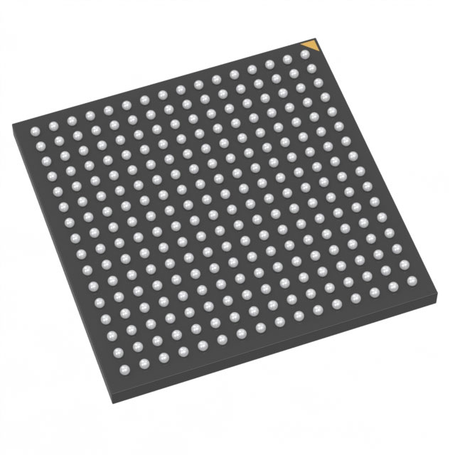
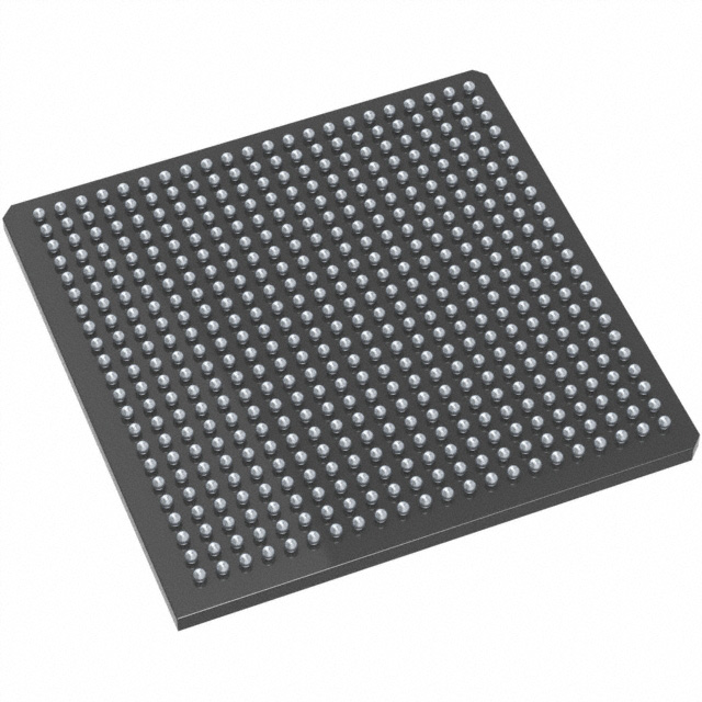
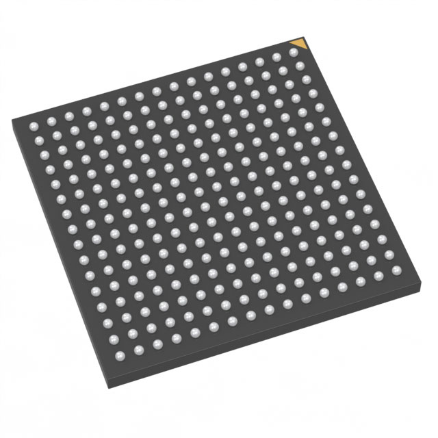
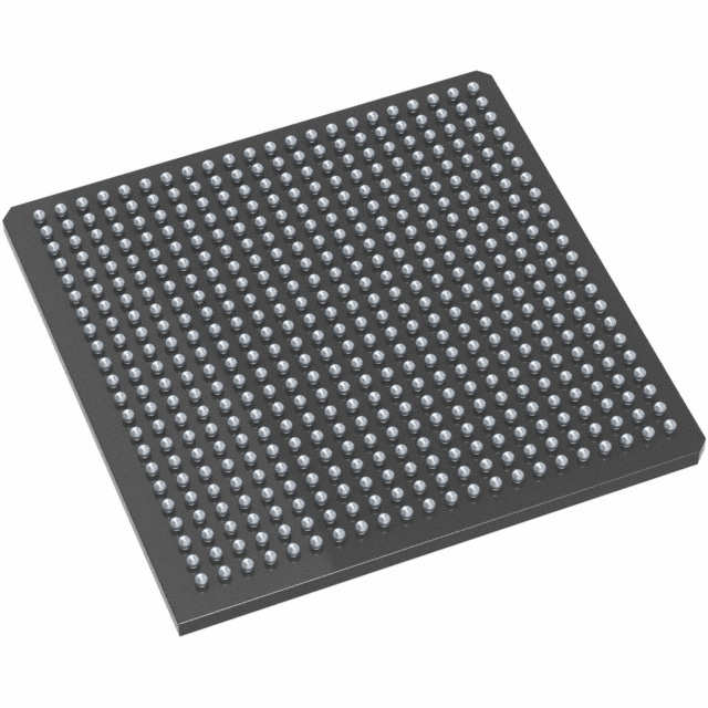
Fusion® Field Programmable Gate Array (FPGA) IC 252 276480 676-BGA |
|---|---|
| Quantity | 662 Available (as of October 7, 2026) |

| Product Category | Field Programmable Gate Array (FPGA) |
|---|---|
| Manufacturer | Microchip Technology |
| Manufacturing Status | Active |
| Manufacturer Standard Lead Time | 52 Weeks |
| Datasheet |
Specifications & Environmental
| Device Package | 676-FBGA (27x27) | Grade | Commercial | Operating Temperature | 0°C – 85°C | ||
|---|---|---|---|---|---|---|---|
| Package / Case | 676-BGA | Number of I/O | 252 | Voltage | 1.425 V - 1.575 V | ||
| Mounting Method | Surface Mount | RoHS Compliance | RoHS non-compliant | REACH Compliance | REACH Unaffected | ||
| Moisture Sensitivity Level | 3 (168 Hours) | Number of LABs/CLBs | 38400 | Number of Logic Elements/Cells | 38400 | ||
| Number of Gates | 1500000 | ECCN | 3A991D | HTS Code | 8542.39.0001 | ||
| Qualification | N/A | Total RAM Bits | 276480 |
Overview of M1AFS1500-FG676 – Fusion® Field Programmable Gate Array, 676-BGA, 252 I/O
The M1AFS1500-FG676 is a Fusion® Field Programmable Gate Array (FPGA) from Microchip Technology supplied in a 676-ball BGA package. It is a high-density, commercial-grade programmable logic device offering a balance of logic capacity, embedded memory, and a substantial I/O count for complex custom logic integration.
Targeted at commercial embedded and system designs, this FPGA provides designers with a compact, surface-mount solution for applications requiring up to 252 I/O, about 38,400 logic elements, and on-chip memory to implement custom logic, glue logic, and interface functions.
Key Features
- Core Logic Approximately 38,400 logic elements offering a sizeable programmable fabric for custom combinational and sequential logic implementations.
- Gate Density Approximately 1,500,000 gates to support complex logic architectures and moderate-scale system functions.
- Embedded Memory Approximately 0.276 Mbits of on-chip RAM (276,480 total RAM bits) for buffering, small lookup tables, and temporary data storage within user logic.
- I/O Capacity 252 I/O pins to support multiple parallel interfaces, sensor arrays, or mixed-signal front-end routing when used with appropriate external components.
- Package 676-FBGA (27 × 27 mm) surface-mount package for compact board-level integration and high pin density.
- Power Specified supply voltage range of 1.425 V to 1.575 V to match system power domains and design requirements.
- Commercial Temperature & Mounting Rated for 0 °C to 85 °C operating temperature and designed for surface-mount PCB assembly in commercial applications.
- Compliance RoHS compliant, supporting environmental regulatory requirements for lead-free assembly.
Typical Applications
- Commercial Embedded Systems Implement custom control logic, protocol bridging, or peripheral aggregation using the device's logic capacity and 252 I/O lines.
- Prototyping and Development Rapidly validate hardware architectures and accelerate time-to-prototype with a programmable fabric sized for mid-range designs.
- High-density Interface Aggregation Consolidate multiple parallel interfaces or I/O channels on a single device to reduce board-level complexity.
Unique Advantages
- High Logic Capacity: Approximately 38,400 logic elements and 1,500,000 gates enable implementation of substantial custom logic without excessive external components.
- Built-in On-chip Memory: About 0.276 Mbits of embedded RAM reduces the need for small external buffers and eases data-path design within the FPGA fabric.
- Generous I/O Count: 252 I/O pins support diverse peripheral connections and parallel interfacing for system integration.
- Compact, High-density Package: 676-FBGA (27 × 27 mm) provides high pin density in a compact form factor for space-constrained PCBs.
- Commercial-ready Operating Range: Rated for 0 °C to 85 °C, suitable for a wide range of commercial applications where this temperature range is required.
- RoHS Compliant: Meets lead-free assembly requirements for modern manufacturing processes.
Why Choose M1AFS1500-FG676?
The M1AFS1500-FG676 positions itself as a mid-to-high-density Fusion® FPGA option for commercial embedded designs that need a combination of substantial programmable logic, embedded memory, and a large I/O complement in a compact BGA package. Its specified supply voltage range and RoHS compliance make it suitable for modern PCB assembly and system power domains.
This device is well suited to designers and OEMs building commercial products that require flexible hardware programmability, interface consolidation, and scalable logic capacity. It offers long-term design flexibility by enabling functionality updates and iterative hardware refinement through reprogrammable logic.
Request a quote or submit an inquiry to get pricing and availability information for the M1AFS1500-FG676 from Microchip Technology sales channels.




















Date Founded: 1989
Headquarters: Chandler, Arizona, USA
Employees: 22,000+
Revenue: $8.349 Billion
Certifications and Memberships: ISO9001:2015, IATF16949:2016, AS 9100D




