
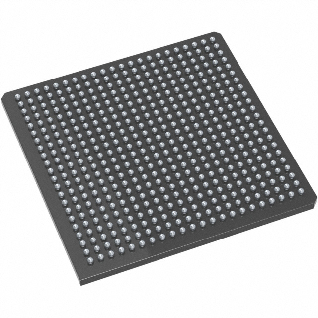
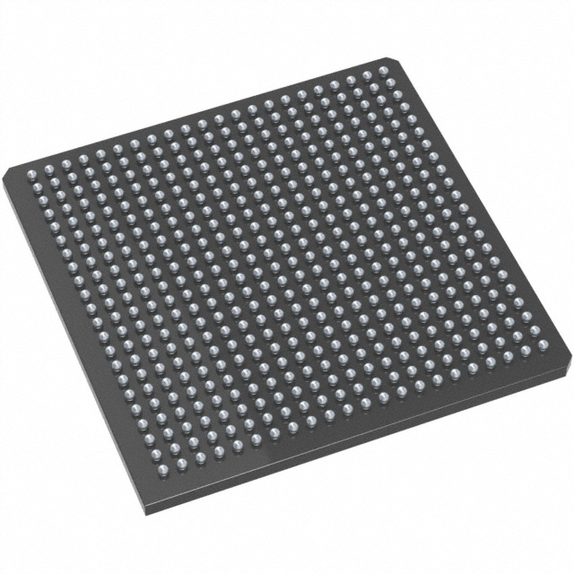
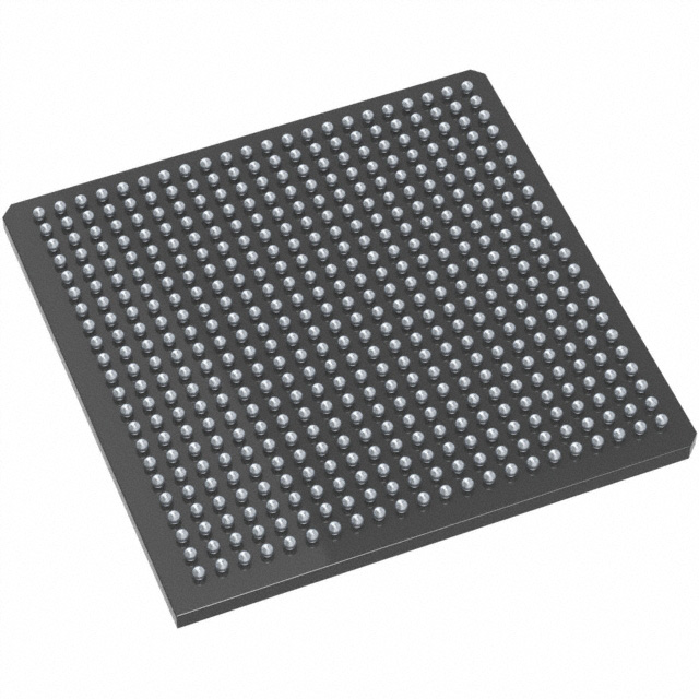
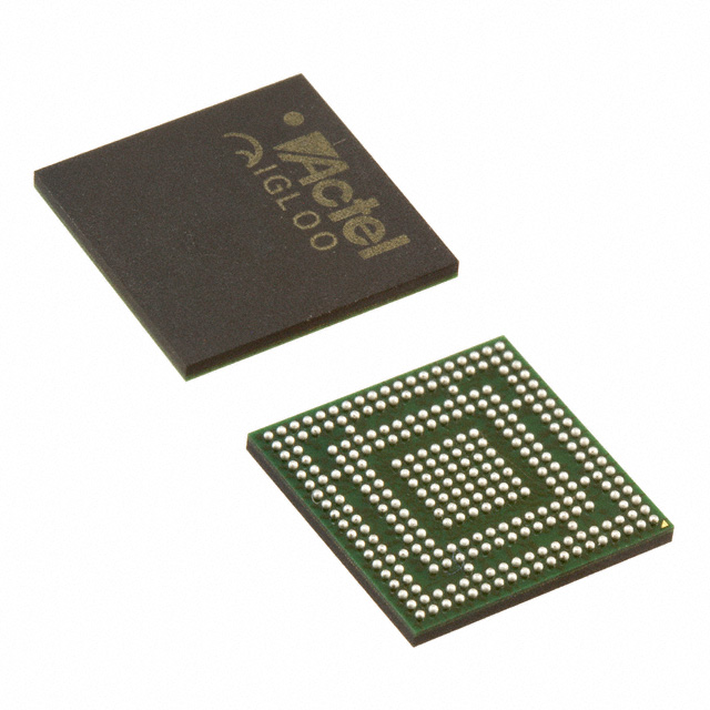
M1AFS600-FGG484
| Part Description |
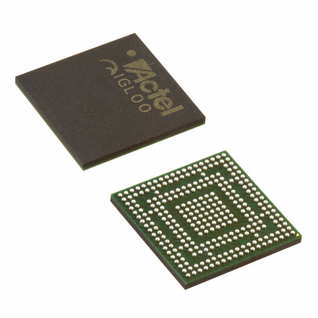
Fusion® Field Programmable Gate Array (FPGA) IC 172 110592 484-BGA |
|---|---|
| Quantity | 296 Available (as of October 8, 2026) |
| Product Category | Field Programmable Gate Array (FPGA) |
|---|---|
| Manufacturer | Microchip Technology |
| Manufacturing Status | Active |
| Manufacturer Standard Lead Time | 16 Weeks |
| Datasheet |
Specifications & Environmental
| Device Package | 484-FPBGA (23x23) | Grade | Commercial | Operating Temperature | 0°C – 85°C | ||
|---|---|---|---|---|---|---|---|
| Package / Case | 484-BGA | Number of I/O | 172 | Voltage | 1.425 V - 1.575 V | ||
| Mounting Method | Surface Mount | RoHS Compliance | ROHS3 Compliant | REACH Compliance | REACH Unaffected | ||
| Moisture Sensitivity Level | 3 (168 Hours) | Number of LABs/CLBs | 13824 | Number of Logic Elements/Cells | 13824 | ||
| Number of Gates | 600000 | ECCN | 3A991D | HTS Code | 8542.39.0001 | ||
| Qualification | N/A | Total RAM Bits | 110592 |
Overview of M1AFS600-FGG484 – Fusion® Field Programmable Gate Array (FPGA) IC 172 110592 484-BGA
The M1AFS600-FGG484 is a Fusion® Field Programmable Gate Array from Microchip Technology, delivered in a 484-ball BGA (23×23) package for surface-mount assembly. It provides a mid-density programmable logic resource with 13,824 logic elements and approximately 0.11 Mbits of embedded memory, suitable for commercial applications requiring configurable logic, parallel I/O, and on-chip RAM.
With 172 I/O pins, 600,000 gates and a defined core supply range of 1.425 V to 1.575 V, this device targets designers who need a balance of integration and predictable operating parameters within a commercial temperature range (0 °C to 85 °C).
Key Features
- Core Logic 13,824 logic elements (cells) and 600,000 gates provide mid-range programmable logic capacity for custom digital functions and control logic.
- Embedded Memory Approximately 0.11 Mbits of on-chip RAM (110,592 total RAM bits) supports local buffering, small lookup tables, and state storage without external memory.
- I/O Resources 172 I/O pins deliver broad interfacing capability for parallel peripherals, sensors, and external devices in a single-package solution.
- Power Specified core voltage supply from 1.425 V to 1.575 V enables deterministic power planning and integration into systems with tightly controlled supply rails.
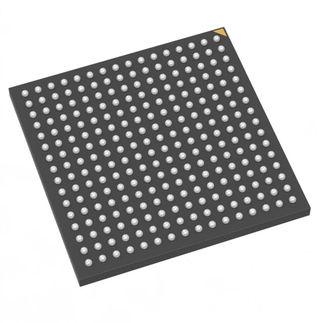
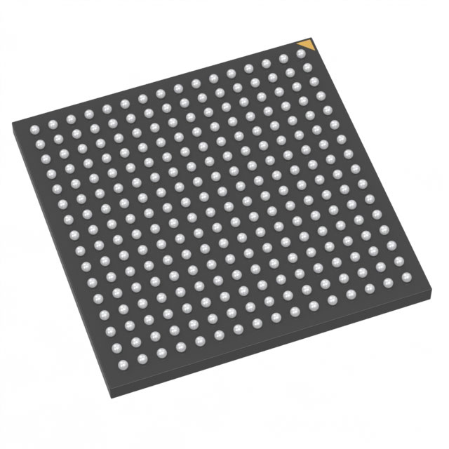
- Package & Mounting 484‑ball FPBGA (23×23) package in surface-mount format provides a compact, high-density footprint for space-constrained PCBs.
- Operating Conditions Commercial grade device rated for 0 °C to 85 °C ambient operation and RoHS-compliant construction for regulatory compatibility.
Typical Applications
- Embedded Control Implement custom control algorithms and glue logic for commercial electronic products requiring configurable finite-state machines and timing control.
- Interface Bridging Aggregate and translate signals between multiple parallel or serial interfaces using the device’s abundant I/O resources.
- Prototyping and Development Use as a flexible hardware platform for validating digital designs, integrating small on-chip memory and reprogrammable logic for iterative development.
Unique Advantages
- Balanced Logic Capacity: 13,824 logic elements and 600,000 gates deliver substantial programmable resources without the complexity or cost of higher-end devices.
- Integrated On‑Chip Memory: Approximately 0.11 Mbits of RAM reduces dependence on external memory for small buffers and state storage, simplifying board design.
- Generous I/O Count: 172 I/O pins enable direct connection to multiple peripherals and parallel buses, reducing the need for external I/O expanders.
- Compact BGA Package: 484-ball FPBGA (23×23) offers high pin density in a compact footprint, helping conserve PCB area in space-constrained designs.
- Predictable Power Envelope: A clearly defined core supply range (1.425 V–1.575 V) aids in power supply selection and system integration.
- Commercial Temperature Rating: Rated for 0 °C to 85 °C operation, suitable for a wide range of commercial electronic products.
Why Choose M1AFS600-FGG484?
The M1AFS600-FGG484 positions itself as a mid-density, commercial-grade FPGA that combines a practical number of logic elements, on-chip RAM, and a high I/O count in a compact 484‑BGA package. It is well suited for designers who require reconfigurable logic and local memory in commercial electronic systems where board space and predictable supply requirements matter.
Backed by Microchip Technology, this Fusion® device offers a clear, specification-driven option for projects that need moderate programmable capacity with deterministic operating parameters and RoHS-compliant construction.
Request a quote or submit a purchase inquiry to obtain pricing, lead time, and availability for the M1AFS600-FGG484. Provide your project requirements to receive tailored order information and support.





















Date Founded: 1989
Headquarters: Chandler, Arizona, USA
Employees: 22,000+
Revenue: $8.349 Billion
Certifications and Memberships: ISO9001:2015, IATF16949:2016, AS 9100D




