
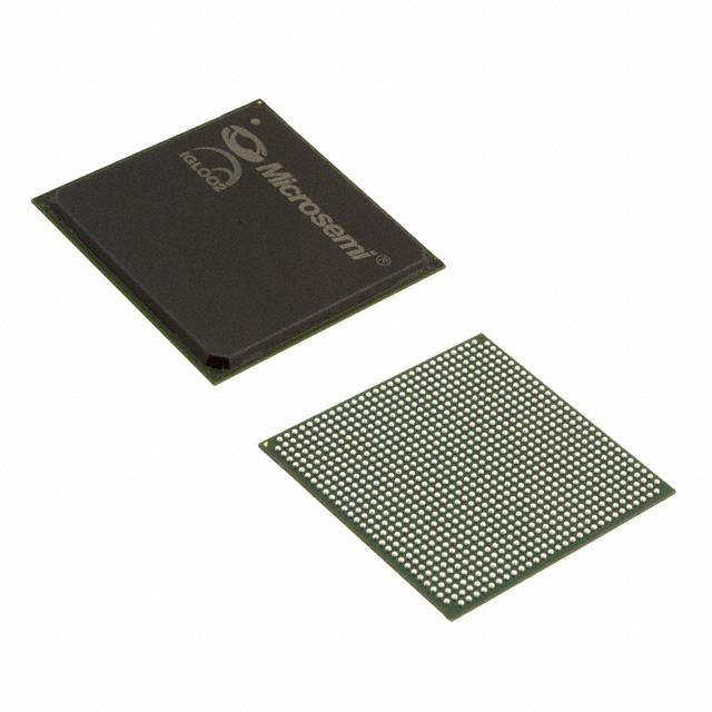
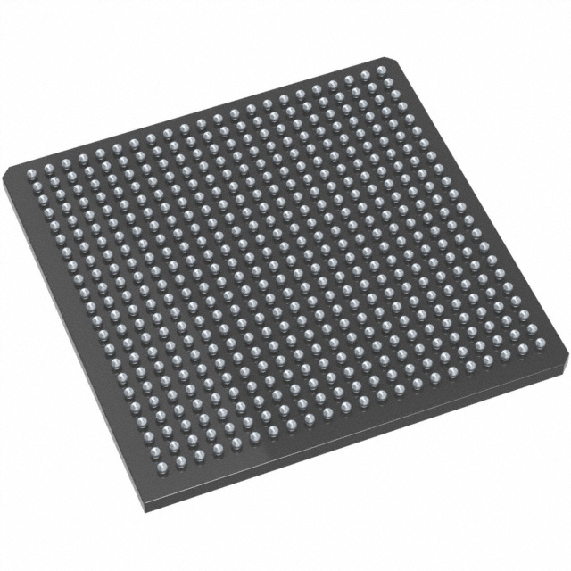
M2GL050T-1FGG484
| Part Description |
IGLOO2 Field Programmable Gate Array (FPGA) IC 267 1869824 56340 484-BGA |
|---|---|
| Quantity | 1,203 Available (as of June 15, 2026) |

| Product Category | Field Programmable Gate Array (FPGA) |
|---|---|
| Manufacturer | Microchip Technology |
| Manufacturing Status | Active |
| Manufacturer Standard Lead Time | 16 Weeks |
| Datasheet |
Specifications & Environmental
| Device Package | 484-FPBGA (23x23) | Grade | Commercial | Operating Temperature | 0°C – 85°C | ||
|---|---|---|---|---|---|---|---|
| Package / Case | 484-BGA | Number of I/O | 267 | Voltage | 1.14 V - 2.625 V | ||
| Mounting Method | Surface Mount | RoHS Compliance | ROHS3 Compliant | REACH Compliance | REACH Unaffected | ||
| Moisture Sensitivity Level | 3 (168 Hours) | Number of LABs/CLBs | 56340 | Number of Logic Elements/Cells | 56340 | ||
| Number of Gates | N/A | ECCN | 3A991D | HTS Code | 8542.39.0001 | ||
| Qualification | N/A | Total RAM Bits | 1869824 |
Overview of M2GL050T-1FGG484 – IGLOO2 Field Programmable Gate Array (484-BGA)
The M2GL050T-1FGG484 is a Microchip Technology IGLOO2 flash-based FPGA in a 484-ball BGA package. It integrates fourth-generation flash FPGA fabric with high-performance communications and memory interfaces, delivering a balance of programmable logic, embedded memory, I/O density, and security features for embedded and communications-focused designs.
This device provides 56,340 logic elements, approximately 1.87 Mbits of on-chip RAM, and 267 user I/Os, and operates from a 1.14 V to 2.625 V supply over a commercial temperature range of 0 °C to 85 °C in a 23 × 23 mm 484-FPBGA surface-mount package.
Key Features
- Programmable Fabric Efficient 4-input LUT architecture with carry chains for enhanced arithmetic performance and general logic implementation.
- Logic Capacity 56,340 logic elements suitable for mid-range FPGA designs requiring substantial programmable resources.
- Embedded Memory Approximately 1.87 Mbits of total on-chip RAM with family-level options including large dual-port SRAM blocks and three-port micro SRAM for flexible memory partitioning and buffering.
- DSP / Mathblocks Mathblock support for signed/unsigned multiplication and accumulation to accelerate DSP and arithmetic-heavy functions.
- High-Speed Serial Interfaces Family support for up to 16 SERDES lanes and protocol support including PCI Express (x1/x2/x4) and XGMII/XAUI-style interfaces for high-throughput link designs.
- High-Speed Memory Controllers On-chip controllers support LPDDR/DDR2/DDR3 memory interfaces with family-level clocking to 333 MHz and multiple DRAM bus widths.
- Clocking Resources Multiple clock sources and up to eight Clock Conditioning Circuits (CCCs) with integrated PLLs to generate and manage system clocks across domains.
- Multi-Standard I/Os Support for a wide range of I/O standards (LVCMOS, LVDS variants, DDR I/Os, SSTL, etc.) and a high user I/O count (267) for dense peripheral connectivity.
- Security and Reliability Family-level design and data security features including encrypted bitstream support, anti-tamper/zeroization capabilities, and optional cryptographic primitives for protected implementations.
- Package & Environmental 484-FPBGA (23×23) surface-mount package, commercial grade, RoHS compliant, and specified for 0 °C to 85 °C operation.
Typical Applications
- High-Speed Networking: Use SERDES lanes and PCIe endpoint capability to implement Ethernet PHY extensions, packet processing, or network interface functions.
- Memory-Intensive Embedded Systems: Leverage on-chip RAM and DDRx controllers to manage buffering, frame storage, and high-bandwidth memory access in embedded platforms.
- Signal Processing and DSP: Deploy mathblocks and fast embedded memory for real-time DSP tasks such as filtering, FFTs, or sample-rate conversion.
- Secure Embedded Controllers: Use encrypted bitstream support and anti-tamper features to protect IP and data in secure system designs.
- High-Density I/O Interfaces: Apply the 267 user I/Os and multi-standard I/O support for complex sensor aggregation, control interfaces, and peripheral bridging.
Unique Advantages
- Flash-Based Nonvolatile Fabric: Fourth-generation flash-based FPGA fabric enables nonvolatile configuration and stable power-up behavior for field-deployable systems.
- Balanced Performance and Integration: Combines sizable logic capacity, embedded RAM, DSP mathblocks, and high-speed serial links in a single 484-BGA package to reduce system BOM and board area.
- Flexible Memory Subsystem: On-chip SRAM blocks, eSRAM/eNVM family options, and DDRx controllers support diverse memory architectures and buffering strategies.
- High I/O Density: 267 user I/Os with multi-standard support facilitate broad peripheral connectivity without external translators.
- Security-Ready Features: Encrypted bitstream loading, anti-tamper capabilities, and optional cryptographic primitives support secure deployment models.
- Commercial Temperature and RoHS Compliance: Commercial-grade rating (0 °C to 85 °C) and RoHS compliance accommodate a wide range of mainstream embedded applications.
Why Choose M2GL050T-1FGG484?
The M2GL050T-1FGG484 targets designs that require a balanced mix of programmable logic, on-chip memory, DSP acceleration, dense I/O, and high-speed serial connectivity in a single, flash-based FPGA. Its IGLOO2 architecture brings family-level capabilities—such as configurable DDR controllers, SERDES lanes, and built-in security features—into a compact 484-BGA package suited for commercial embedded and communications applications.
Designers seeking a scalable, secure, and integrated programmable solution will find this device well suited for mid-range FPGA roles where reliable nonvolatile configuration, flexible memory interfacing, and substantial I/O are key selection criteria.
Request a quote or submit an inquiry to receive pricing and availability information for the M2GL050T-1FGG484.


Date Founded: 1989
Headquarters: Chandler, Arizona, USA
Employees: 22,000+
Revenue: $8.349 Billion
Certifications and Memberships: ISO9001:2015, IATF16949:2016, AS 9100D


