
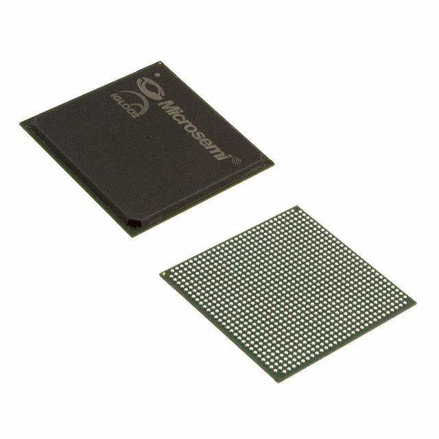
M2GL050T-1FG896I
| Part Description |
IGLOO2 Field Programmable Gate Array (FPGA) IC 377 1869824 56340 896-BGA |
|---|---|
| Quantity | 1,425 Available (as of June 15, 2026) |

| Product Category | Field Programmable Gate Array (FPGA) |
|---|---|
| Manufacturer | Microchip Technology |
| Manufacturing Status | Active |
| Manufacturer Standard Lead Time | 16 Weeks |
| Datasheet |
Specifications & Environmental
| Device Package | 896-FBGA (31x31) | Grade | Industrial | Operating Temperature | -40°C – 100°C | ||
|---|---|---|---|---|---|---|---|
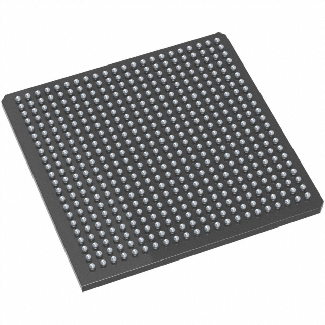
| Package / Case | 896-BGA | Number of I/O | 377 | Voltage | 1.14 V - 2.625 V | ||
| Mounting Method | Surface Mount | RoHS Compliance | RoHS non-compliant | REACH Compliance | REACH Unaffected | ||
| Moisture Sensitivity Level | 3 (168 Hours) | Number of LABs/CLBs | 56340 | Number of Logic Elements/Cells | 56340 | ||
| Number of Gates | N/A | ECCN | 3A991D | HTS Code | 8542.39.0001 | ||
| Qualification | N/A | Total RAM Bits | 1869824 |
Overview of M2GL050T-1FG896I – IGLOO2 Field Programmable Gate Array, 377 I/Os, 896‑BGA
The M2GL050T-1FG896I is an IGLOO2 family flash-based Field Programmable Gate Array (FPGA) IC combining programmable fabric with high-performance communications and memory interfaces. It targets designs that require a balance of logic capacity, embedded memory, secure design features, and flexible I/O in a surface-mount 896‑BGA package.
Built on the IGLOO2 architecture, this device emphasizes low-power operation, integrated DSP and memory options, and high-speed serial and DDR memory interfaces for applications spanning communications, industrial control, and secure embedded systems.
Key Features
- Logic Capacity — 56,340 logic elements provide substantial programmable fabric for complex logic and control functions.
- Embedded Memory — Approximately 1.87 Mbits of on-chip RAM (total RAM bits: 1,869,824) plus embedded SRAM and nonvolatile memory options in the IGLOO2 family architecture.
- High-Performance DSP — Family architecture includes up to 240 Fast Mathblocks for multiply-accumulate and DSP tasks (family-level specification).
- High-Speed Serial and Memory Interfaces — Family-level support for up to 16 SERDES lanes and up to two high-speed DDRx memory controllers (DDR/DDR2/DDR3/LPDDR) with maximum 333 MHz clock rate.
- Flexible I/O Standards — 377 user I/Os supporting multiple standards (LVCMOS, LVDS, DDR I/Os and more as defined by the IGLOO2 family).
- Voltage and Power — Operates across a supply range of 1.14 V to 2.625 V to accommodate varied core and I/O power domains.
- Package and Mounting — Surface-mount 896‑BGA package (supplier device package: 896‑FBGA, 31 × 31 mm) for high-density board designs.
- Industrial Temperature Range — Rated for operation from −40 °C to 100 °C, supporting industrial environments.
- Security and Reliability — IGLOO2 family design security features include encrypted bitstream loading, supply-chain assurance device certificate, anti-tamper capabilities, and optional cryptographic services on premium devices.
- RoHS Compliant — Device is RoHS compliant for environmental and manufacturing requirements.
Typical Applications
- High-Speed Communications — Use the device where SERDES lanes and PCIe/XAUI-capable interfaces are needed for PHY-level or protocol bridging tasks.
- Memory-Intensive Systems — Leverage integrated DDRx controllers and substantial on-chip RAM for buffering, packet aggregation, or frame storage in networking and data-handling designs.
- Signal Processing — Apply the embedded DSP/mathblock capabilities for real-time filtering, aggregation, or other digital signal processing workloads.
- Industrial Control and Automation — Deploy in control logic, sensor interfacing, and deterministic I/O applications benefitting from the device’s industrial temperature rating and flexible I/O standards.
- Security-Sensitive Embedded Systems — Utilize encrypted bitstream loading and device-level security features for systems requiring supply-chain assurance and anti-tamper measures.
Unique Advantages
- High Logic Density: 56,340 logic elements enable implementation of complex state machines, protocol stacks, and glue logic in a single device, reducing board-level complexity.
- Integrated Memory Resources: Approximately 1.87 Mbits of on-chip RAM plus family-level embedded SRAM and nonvolatile memory options simplify memory architecture and accelerate data paths.
- Flexible, High-Speed I/O: 377 user I/Os combined with family support for SERDES and DDRx controllers provide a broad interface palette for mixed-signal and high-throughput designs.
- Industrial-Grade Operation: −40 °C to 100 °C rating and surface-mount 896‑BGA packaging suit demanding environmental and density requirements.
- Security-Ready Architecture: Built-in encrypted bitstream loading, supply-chain assurance, and optional cryptographic primitives support secure deployment and IP protection.
- Low-Voltage Flexibility: Wide supply range (1.14 V to 2.625 V) supports varied power domains and modern low-voltage system requirements.
Why Choose M2GL050T-1FG896I?
The M2GL050T-1FG896I delivers a balanced blend of programmable logic density, embedded memory, DSP capability, and high-speed interfaces within a secure IGLOO2 architecture. Its combination of 56,340 logic elements, approximately 1.87 Mbits of on-chip RAM, 377 user I/Os, and industrial temperature rating makes it well-suited for communications, industrial, and security-conscious embedded designs.
Designers seeking a low-power, flash-based FPGA with family-level support for SERDES, DDRx memory controllers, and advanced security mechanisms will find the M2GL050T-1FG896I appropriate for scalable, robust implementations that reduce BOM complexity and support long-term deployment.
Request a quote or submit an inquiry for pricing and availability of the M2GL050T-1FG896I to begin integrating this IGLOO2 FPGA into your next design.


Date Founded: 1989
Headquarters: Chandler, Arizona, USA
Employees: 22,000+
Revenue: $8.349 Billion
Certifications and Memberships: ISO9001:2015, IATF16949:2016, AS 9100D


