
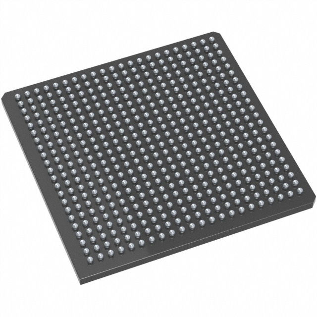
M2GL060TS-1FG484M
| Part Description |
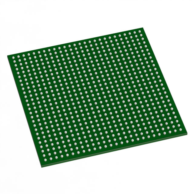
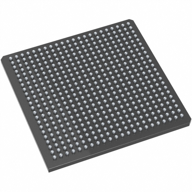
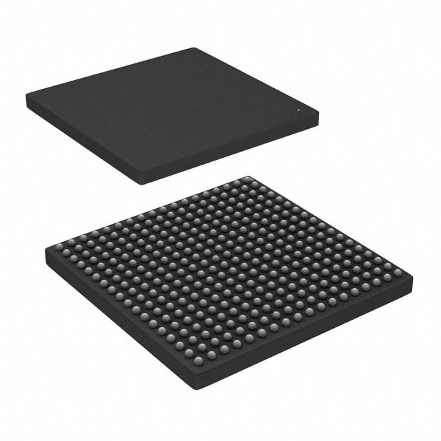
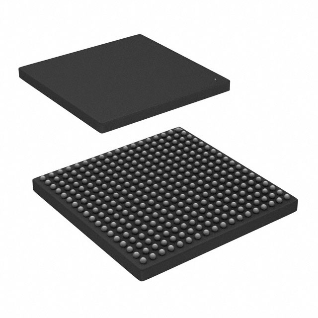
IGLOO2 Field Programmable Gate Array (FPGA) IC 267 1869824 56520 484-BGA |
|---|---|
| Quantity | 1,787 Available (as of October 8, 2026) |
| Product Category | Field Programmable Gate Array (FPGA) |
|---|---|
| Manufacturer | Microchip Technology |
| Manufacturing Status | Active |
| Manufacturer Standard Lead Time | 16 Weeks |
| Datasheet |
Specifications & Environmental
| Device Package | 484-FPBGA (23x23) | Grade | Military | Operating Temperature | -55°C – 125°C | ||
|---|---|---|---|---|---|---|---|
| Package / Case | 484-BGA | Number of I/O | 267 | Voltage | 1.14 V - 2.625 V | ||
| Mounting Method | Surface Mount | RoHS Compliance | RoHS non-compliant | REACH Compliance | REACH Unaffected | ||
| Moisture Sensitivity Level | 3 (168 Hours) | Number of LABs/CLBs | 56520 | Number of Logic Elements/Cells | 56520 | ||
| Number of Gates | N/A | ECCN | 5A002A1 | HTS Code | 8542.39.0001 | ||
| Qualification | MIL-STD-883 | Total RAM Bits | 1869824 |
Overview of M2GL060TS-1FG484M – IGLOO2 Field Programmable Gate Array (FPGA), 484‑BGA, Military Grade
The M2GL060TS-1FG484M is an IGLOO2-family flash-based FPGA in a 484‑BGA package designed for high-reliability, security-conscious applications. It combines fourth-generation flash FPGA fabric with high-performance communications and memory interfaces to address secure signal processing, high-speed I/O and mission-critical system functions.
With 56,520 logic elements and approximately 1.87 Mbits of embedded RAM, this military‑grade device (MIL‑STD‑883) delivers a balance of integration, low-power operation and robustness across an extended temperature range for demanding embedded systems.
Key Features
- Configurable Logic 56,520 logic elements implemented with efficient 4‑input LUTs and carry chains for high-performance logic synthesis.
- On‑Chip Memory Approximately 1.87 Mbits of total RAM bits plus family support for multiple embedded SRAM configurations to support large buffering and data storage.
- High‑Performance DSP IGLOO2 family mathblocks provide hardware multiplication and accumulation capabilities (series-level DSP resources described in datasheet).
- High‑Speed Serial Interfaces Series-support for up to 16 SERDES lanes enabling protocols such as PCIe and 10 Gbps Ethernet (XGXS/XAUI) as well as native SERDES options.
- High‑Speed Memory Controllers Family-level DDRx controllers (supporting DDR2/DDR3/LPDDR) and up to two high-speed memory controller instances for external DRAM connectivity.
- Security and Tamper Resistance IGLOO2 family security features include encrypted bitstream loading, device certificates and anti‑tamper/zeroization capabilities; premium devices offer cryptographic accelerators and PUF support.
- System Integration Embedded system resources from the series include eSRAM, eNVM, DMA controllers and multi-layer bus matrices for efficient system-level data movement.
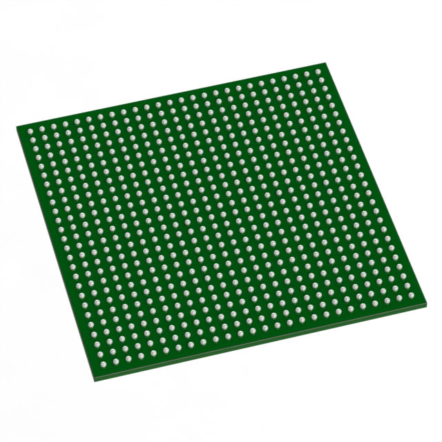
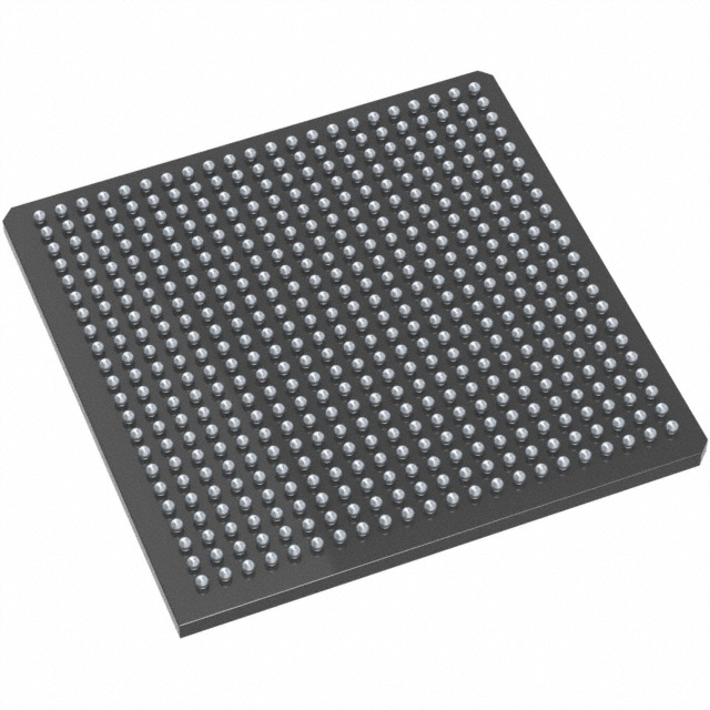
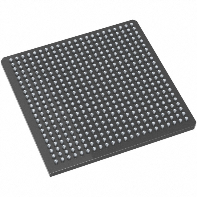
- Package and I/O 484‑BGA (supplier package 484‑FPBGA, 23×23) with 267 I/Os, surface‑mount construction and multi‑standard I/O support detailed at the series level.
- Voltage and Temperature Supported supply range of 1.14 V to 2.625 V and operating temperature range of −55 °C to 125 °C suitable for military environments.
- Qualification & Compliance Military grade device qualified to MIL‑STD‑883 and RoHS compliant.
Typical Applications
- Defense & Aerospace Systems Use for secure, mission‑critical signal processing, data aggregation and control where MIL‑STD‑883 qualification and extended temperature operation are required.
- Secure Communications High‑speed SERDES lanes and PCIe/10Gb Ethernet support enable implementation of secure data links and protocol bridges.
- High‑Performance Embedded Processing DSP mathblocks and substantial on‑chip memory make the device suitable for real‑time processing tasks such as radar, imaging or sensor fusion.
- Memory‑Intensive Control Systems Integrated DDRx controller support and embedded SRAM/eNVM resources simplify designs that require large external memory interfaces and deterministic buffering.
Unique Advantages
- Military‑Qualified Reliability: MIL‑STD‑883 qualification and −55 °C to 125 °C operation support deployment in harsh, mission‑critical environments.
- High Logic and Memory Density: 56,520 logic elements and approximately 1.87 Mbits of on‑chip RAM provide the capacity for complex algorithms and large data structures without immediate dependence on external logic.
- Integrated High‑Speed I/O: Series-level SERDES and PCIe/Ethernet interface capability reduce external PHY and bridge components for cleaner board design and lower BOM.
- Security‑Focused Architecture: Encrypted bitstream loading, device certificates and anti‑tamper features enable secure deployment and supply‑chain assurance.
- Flexible Power and I/O Standards: Broad supply voltage window (1.14 V to 2.625 V) and multi‑standard I/O options support a variety of system voltage domains and memory interfaces.
Why Choose M2GL060TS-1FG484M?
The M2GL060TS-1FG484M brings IGLOO2 family capabilities—flash-based, low-power FPGA fabric with advanced I/O and memory subsystems—into a military‑grade, surface‑mount 484‑BGA package. Its combination of high logic density, embedded memory and series-level communications features makes it well suited for secure, high‑performance embedded designs that require extended temperature operation and formal qualification.
This device is ideal for engineers building reliable, secure systems where long-term robustness, on‑chip DSP and high‑speed interfaces reduce system complexity and accelerate integration.
Request a quote or submit an inquiry to check availability, lead times and pricing for the M2GL060TS-1FG484M. Sales and distribution teams can provide additional ordering and support information.





















Date Founded: 1989
Headquarters: Chandler, Arizona, USA
Employees: 22,000+
Revenue: $8.349 Billion
Certifications and Memberships: ISO9001:2015, IATF16949:2016, AS 9100D




