
M2GL090TS-FCS325
| Part Description |
IGLOO2 Field Programmable Gate Array (FPGA) IC 180 2648064 86184 325-TFBGA, FCBGA |
|---|---|
| Quantity | 334 Available (as of June 18, 2026) |

| Product Category | Field Programmable Gate Array (FPGA) |
|---|---|
| Manufacturer | Microchip Technology |
| Manufacturing Status | Active |
| Manufacturer Standard Lead Time | 10 Weeks |
| Datasheet |
Specifications & Environmental
| Device Package | 325-FCBGA (11x11) | Grade | Commercial | Operating Temperature | 0°C – 85°C | ||
|---|---|---|---|---|---|---|---|
| Package / Case | 325-TFBGA, FCBGA | Number of I/O | 180 | Voltage | 1.14 V - 2.625 V | ||
| Mounting Method | Surface Mount | RoHS Compliance | RoHS non-compliant | REACH Compliance | REACH Unaffected | ||
| Moisture Sensitivity Level | 3 (168 Hours) | Number of LABs/CLBs | 86184 | Number of Logic Elements/Cells | 86184 | ||
| Number of Gates | N/A | ECCN | 3A991B2 | HTS Code | 8542.39.0001 | ||
| Qualification | N/A | Total RAM Bits | 2648064 |
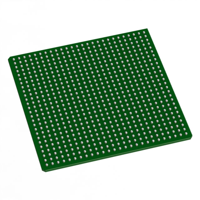
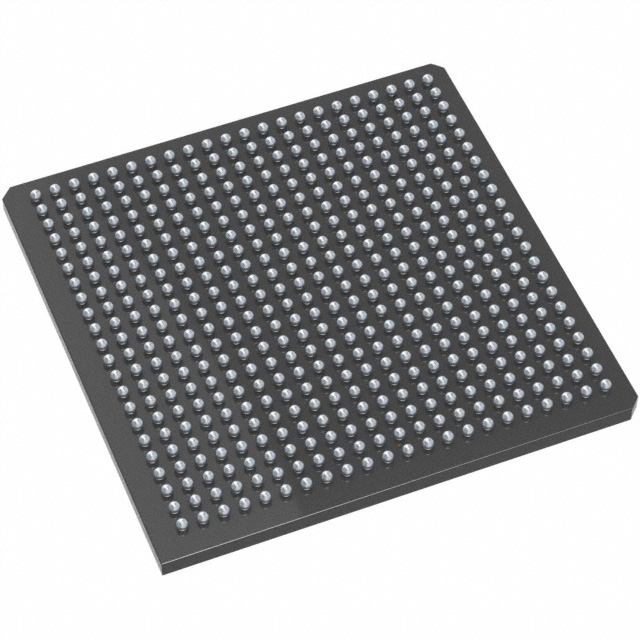
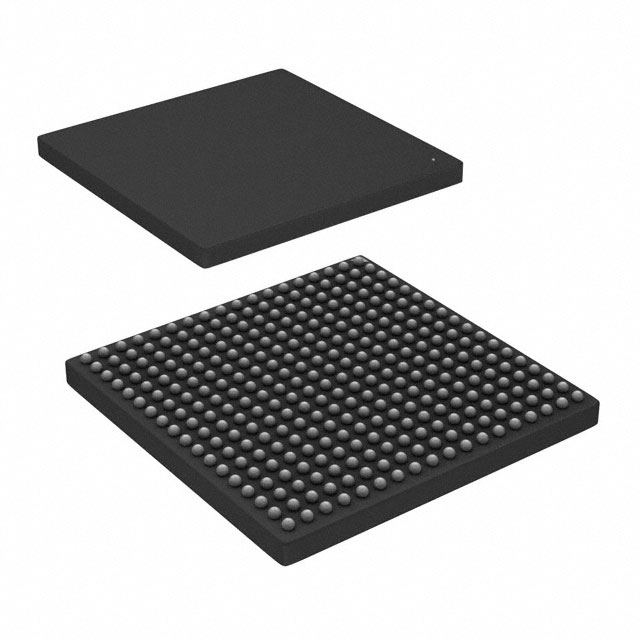
Overview of M2GL090TS-FCS325 – IGLOO2 FPGA, 86,184 logic elements, 325‑TFBGA
The M2GL090TS-FCS325 is an IGLOO2 Field Programmable Gate Array (FPGA) IC from Microchip Technology, delivered in a 325‑TFBGA (11×11) surface-mount package. This commercial‑grade FPGA provides high logic density and embedded memory in a compact, low‑power footprint for board‑level digital designs.
With 86,184 logic elements, approximately 2.65 Mbits of embedded RAM, and 180 I/O pins, the device is suited to designs that require substantial on‑chip logic and memory resources while operating across a 1.14 V to 2.625 V supply range and a 0 °C to 85 °C operating temperature.
Key Features
- Core Logic 86,184 logic elements provide a large fabric for implementing custom digital logic and complex state machines.
- On‑chip Memory Approximately 2.65 Mbits of embedded memory supports buffering, local storage, and data manipulation without external RAM.
- I/O Density 180 general-purpose I/O pins enable broad peripheral interfacing and board connectivity for mixed-signal and digital systems.
- Power and Voltage Flexibility Supports a supply range from 1.14 V to 2.625 V to accommodate various core and I/O voltage schemes.
- Package & Mounting 325‑TFBGA (FCBGA) package, supplier device package 325‑FCBGA (11×11), designed for surface-mount assembly on compact PCBs.
- Operating Range & Grade Commercial grade with an operating temperature range of 0 °C to 85 °C.
- Environmental Compliance RoHS compliant for markets and designs requiring lead-free assembly.
Typical Applications
- Custom Digital Logic and Prototyping Use the FPGA fabric and abundant logic elements to implement custom state machines, accelerators, and prototype systems on a single device.
- Embedded Memory‑Centric Designs Designs that require on‑chip buffering, FIFO implementations, or localized lookup tables can leverage approximately 2.65 Mbits of embedded RAM.
- High‑Pin‑Count Board Solutions With 180 I/O pins and a compact 325‑TFBGA package, the part fits dense board layouts where multiple interfaces and peripherals are needed.
Unique Advantages
- High Logic Density: 86,184 logic elements provide capacity for complex functions and integration of multiple subsystems into one device, reducing external components.
- Substantial On‑Chip RAM: Approximately 2.65 Mbits of embedded memory lowers dependence on external memory, improving performance and simplifying board routing.
- Versatile I/O Count: 180 I/O pins allow flexible interfacing options for sensors, peripherals, and system buses without needing multiple devices.
- Compact Surface‑Mount Package: 325‑TFBGA (11×11) enables dense PCB integration and small form-factor designs while supporting standard surface-mount assembly.
- Wide Supply Range: Support for 1.14 V to 2.625 V supplies offers adaptability to different core and I/O voltage domains.
- Commercial Temperature Rating: 0 °C to 85 °C operation suits a broad range of commercial and consumer applications.
Why Choose M2GL090TS-FCS325?
The M2GL090TS-FCS325 IGLOO2 FPGA combines a high count of logic elements, substantial embedded memory, and a large I/O complement in a compact 325‑TFBGA surface‑mount package. Its electrical and thermal specifications make it well suited to commercial embedded systems that require integrated digital logic, on‑chip storage, and flexible interfacing while maintaining a small board footprint.
Designers seeking scalability and reduced BOM can leverage the device’s integration to consolidate functions into a single FPGA. The combination of logic density, embedded RAM, and I/O capability offers a platform for mid‑to‑high complexity designs where on‑board integration and compact packaging matter.
Request a quote or submit a product inquiry to receive pricing and availability information for the M2GL090TS-FCS325.


Date Founded: 1989
Headquarters: Chandler, Arizona, USA
Employees: 22,000+
Revenue: $8.349 Billion
Certifications and Memberships: ISO9001:2015, IATF16949:2016, AS 9100D


