
M2GL090TS-1FGG676T2
| Part Description |
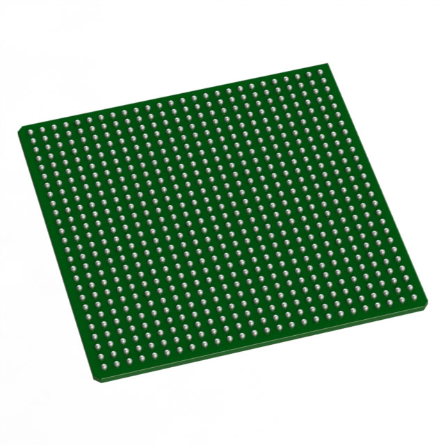
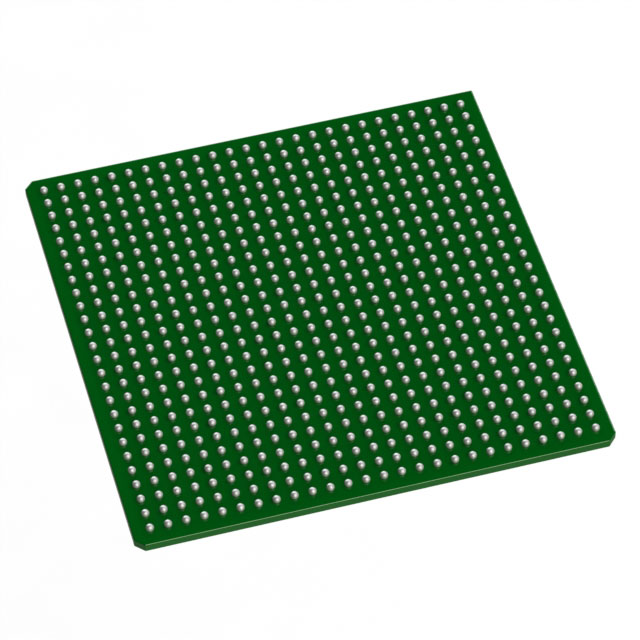
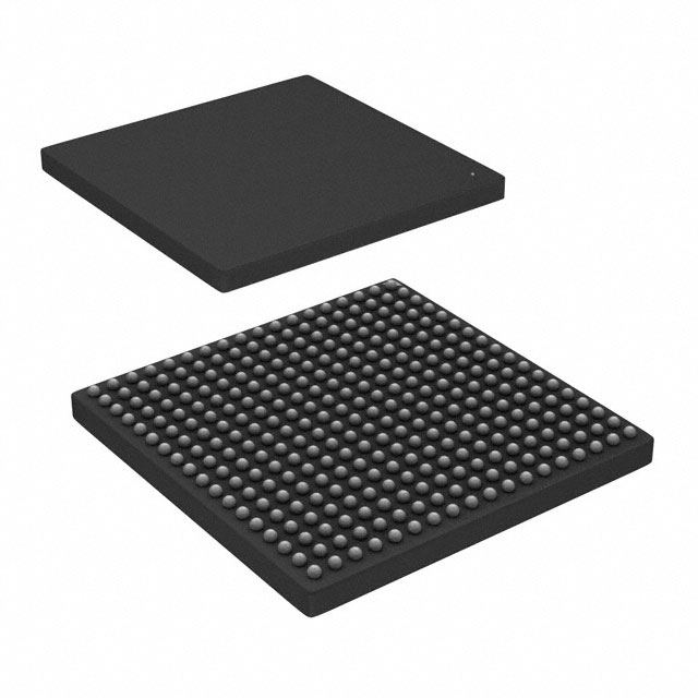
IGLOO2 Field Programmable Gate Array (FPGA) IC 425 2648064 86316 676-BGA |
|---|---|
| Quantity | 1,373 Available (as of October 8, 2026) |
| Product Category | Field Programmable Gate Array (FPGA) |
|---|---|
| Manufacturer | Microchip Technology |
| Manufacturing Status | Active |
| Manufacturer Standard Lead Time | 16 Weeks |
| Datasheet |
Specifications & Environmental
| Device Package | 676-FBGA (27x27) | Grade | Automotive | Operating Temperature | -40°C – 125°C | ||
|---|---|---|---|---|---|---|---|
| Package / Case | 676-BGA | Number of I/O | 425 | Voltage | 1.14 V - 2.625 V | ||
| Mounting Method | Surface Mount | RoHS Compliance | ROHS3 Compliant | REACH Compliance | REACH Unaffected | ||
| Moisture Sensitivity Level | 3 (168 Hours) | Number of LABs/CLBs | 86184 | Number of Logic Elements/Cells | 86316 | ||
| Number of Gates | N/A | ECCN | 5A002A1 | HTS Code | 8542.39.0001 | ||
| Qualification | AEC-Q100 | Total RAM Bits | 2648064 |
Overview of M2GL090TS-1FGG676T2 – IGLOO2 FPGA, 86,316 Logic Elements, 676‑BGA
The M2GL090TS-1FGG676T2 is a Microchip IGLOO2 family field programmable gate array (FPGA) delivered in a 676‑BGA package. It combines flash‑based FPGA fabric and embedded system resources to address applications that require high logic density, extensive I/O and robust on‑chip memory.
Designed for demanding environments, this device provides 86,316 logic elements, approximately 2.65 Mbits of embedded RAM, up to 425 user I/Os and automotive AEC‑Q100 qualification, making it suitable for high‑reliability communication, signal processing and embedded control systems.
Key Features
- Core Architecture
IGLOO2 flash‑based FPGA fabric with 4‑input LUTs and carry chains (family architecture information from product brief). - Logic Capacity
86,316 logic elements to implement complex custom logic and control functions. - Embedded Memory
Approximately 2.65 Mbits (2,648,064 bits) of on‑chip RAM to support buffers, state storage and local data processing. - I/O and High‑Speed SerDes
Up to 425 user I/Os and family‑level support for high‑speed SERDES lanes and protocols such as PCIe and XAUI/XGMII (per IGLOO2 product brief). - High‑Speed Memory Interfaces
Family features include DDRx memory controller support (LPDDR/DDR2/DDR3), enabling high‑bandwidth external memory interfacing where required. - Package and Mounting
676‑BGA (676‑FBGA, 27 × 27 mm) surface mount package for compact system integration. - Voltage and Power
Accepted supply range from 1.14 V to 2.625 V to accommodate various I/O and core power schemes. - Operating Range and Qualification
Rated for −40 °C to 125 °C operation and AEC‑Q100 qualification (automotive grade). - System Integration
Family product brief documents advanced subsystems such as HPMS peripherals, DMA controllers and embedded nonvolatile memory options for integrated system designs. - Regulatory
RoHS compliant.
Typical Applications
- Automotive Control Systems
AEC‑Q100 qualification and −40 °C to 125 °C temperature range make this FPGA suitable for automotive embedded control, domain controllers and safety‑related subsystems. - High‑Speed Communications
Large I/O count and family support for SERDES lanes, PCIe and XAUI enable implementation of Ethernet, PCIe endpoints and other high‑speed interfaces. - Signal Processing and DSP
Significant logic capacity and embedded RAM support DSP pipelines, filtering and math‑intensive functions referenced in the IGLOO2 family brief. - Embedded Memory‑Intensive Systems
On‑chip RAM plus DDRx controller support provide the bandwidth and local storage needed for buffering, frame processing and data logging.
Unique Advantages
- High Logic Density: 86,316 logic elements allow consolidation of multiple functions into a single device, reducing component count.
- Substantial On‑Chip Memory: Approximately 2.65 Mbits of embedded RAM reduces reliance on external memory for many buffering and state‑storage tasks.
- Automotive Qualification: AEC‑Q100 qualification and extended temperature operation support integration into automotive and other harsh‑environment systems.
- Broad I/O and Interface Flexibility: Up to 425 user I/Os and family‑level high‑speed interface support enable versatile protocol and peripheral implementations.
- Compact, Surface‑Mount Package: 676‑BGA (27 × 27 mm) package enables high‑density board layouts while supporting the device’s pin count and thermal needs.
- Wide Supply Range: 1.14 V to 2.625 V supply window accommodates a range of core and I/O voltage configurations.
Why Choose M2GL090TS-1FGG676T2?
The M2GL090TS‑1FGG676T2 delivers a high‑capacity IGLOO2 FPGA configuration that balances substantial logic and on‑chip memory with extensive I/O and automotive qualification. Its combination of 86,316 logic elements, roughly 2.65 Mbits of embedded RAM and support for high‑speed interfaces positions it for systems that demand integrated control, data movement and signal processing.
This device is well suited to engineers developing automotive electronics, communication endpoints and embedded systems that require a qualified, high‑density programmable logic solution with flexible power and packaging options. The IGLOO2 family architecture details further support integrated subsystem implementation where on‑chip peripherals and memory controllers are required.
Request a quote or submit an inquiry for pricing and availability to begin evaluating the M2GL090TS-1FGG676T2 for your next design.





















Date Founded: 1989
Headquarters: Chandler, Arizona, USA
Employees: 22,000+
Revenue: $8.349 Billion
Certifications and Memberships: ISO9001:2015, IATF16949:2016, AS 9100D




