
M2GL150TS-1FCSG536I
| Part Description |
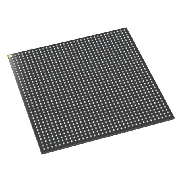
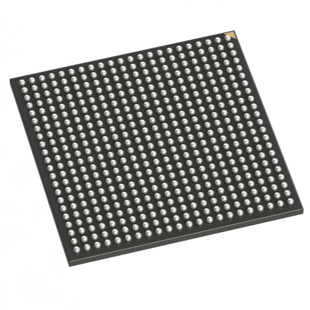
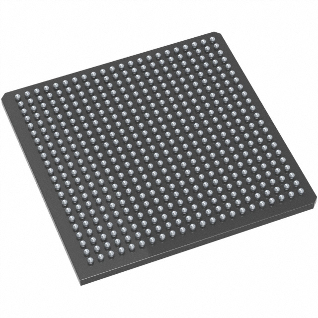
IGLOO2 Field Programmable Gate Array (FPGA) IC 293 5120000 146124 536-LFBGA, CSPBGA |
|---|---|
| Quantity | 531 Available (as of June 18, 2026) |

| Product Category | Field Programmable Gate Array (FPGA) |
|---|---|
| Manufacturer | Microchip Technology |
| Manufacturing Status | Active |
| Manufacturer Standard Lead Time | 10 Weeks |
| Datasheet |
Specifications & Environmental
| Device Package | 536-CSPBGA (16x16) | Grade | Industrial | Operating Temperature | -40°C – 100°C | ||
|---|---|---|---|---|---|---|---|
| Package / Case | 536-LFBGA, CSPBGA | Number of I/O | 293 | Voltage | 1.14 V - 2.625 V | ||
| Mounting Method | Surface Mount | RoHS Compliance | ROHS3 Compliant | REACH Compliance | REACH Unaffected | ||
| Moisture Sensitivity Level | 3 (168 Hours) | Number of LABs/CLBs | 146124 | Number of Logic Elements/Cells | 146124 | ||
| Number of Gates | N/A | ECCN | 3A991B2 | HTS Code | 8542.39.0001 | ||
| Qualification | N/A | Total RAM Bits | 5120000 |
Overview of M2GL150TS-1FCSG536I – IGLOO2 Field Programmable Gate Array (FPGA) IC
The M2GL150TS-1FCSG536I is an IGLOO2 field programmable gate array (FPGA) IC offering a high-density logic fabric in a compact 536‑LFBGA (536‑CSPBGA) package. This industrial-grade device provides 146,124 logic elements, approximately 5.12 Mbits of embedded memory, and 293 user I/Os, delivering on-chip resources for complex reconfigurable designs.
Designed for surface-mount assembly and rated for an operating temperature range of -40 °C to 100 °C, the device supports systems with core supply voltages from 1.14 V to 2.625 V and is RoHS compliant.
Key Features
- Core Logic 146,124 logic elements to implement extensive combinational and sequential logic functions within a single FPGA device.
- On‑Chip Memory Approximately 5.12 Mbits of embedded RAM for buffering, data storage, and tightly coupled memory functions.
- I/O Capacity 293 user I/Os to support broad external interfacing and parallel signal connectivity in mixed-signal and digital systems.
- Power and Supply Operates across a core voltage range of 1.14 V to 2.625 V to match a variety of system power architectures.
- Package and Mounting 536‑LFBGA (536‑CSPBGA, 16×16) package optimized for surface-mount assembly, balancing pin count and board footprint.
- Environmental and Reliability Industrial grade device with an operating temperature range of -40 °C to 100 °C and RoHS compliance for regulatory compatibility.
Typical Applications
- Industrial Control Reconfigurable logic and extensive I/O count support sensor interfacing, motor control, and real-time control functions in industrial automation equipment.
- Data Acquisition and Processing Embedded RAM and large logic capacity enable buffering, pre‑processing, and protocol handling for data acquisition modules.
- Communications and Networking High I/O availability and on‑chip resources allow implementation of custom protocol engines, bridging, and peripheral aggregation.
Unique Advantages
- High Logic Density: 146,124 logic elements provide substantial on-chip implementation capability, reducing the need for multiple discrete devices.
- Substantial Embedded Memory: Approximately 5.12 Mbits of RAM supports local data storage and low-latency buffering for performance-sensitive logic.
- Large I/O Count: 293 user I/Os enable flexible interfacing to sensors, actuators, high-speed peripherals, and parallel buses.
- Industrial Temperature Range: Rated from -40 °C to 100 °C for deployment in temperature‑challenging environments.
- Compact, High‑Pin Package: 536‑CSPBGA (16×16) package concentrates signals and I/O in a manageable footprint for space-constrained boards.
- Regulatory Compliance: RoHS compliance supports environmental and manufacturing requirements.
Why Choose M2GL150TS-1FCSG536I?
The M2GL150TS-1FCSG536I positions itself as a robust industrial-grade FPGA option where substantial logic capacity, on-chip memory, and a high number of I/Os are required in a compact surface-mount package. Its operating voltage range and extended temperature rating make it suitable for designs that demand resilience and configurability.
This device is well suited for engineers and procurement teams building industrial control, data acquisition, and communications systems who need a single FPGA with integrated memory and extensive I/O to simplify board-level design and reduce component count.
Request a quote or submit an inquiry for pricing and availability of the M2GL150TS-1FCSG536I to evaluate it for your next design.


Date Founded: 1989
Headquarters: Chandler, Arizona, USA
Employees: 22,000+
Revenue: $8.349 Billion
Certifications and Memberships: ISO9001:2015, IATF16949:2016, AS 9100D


