
XC2S100-5FGG256C
| Part Description |
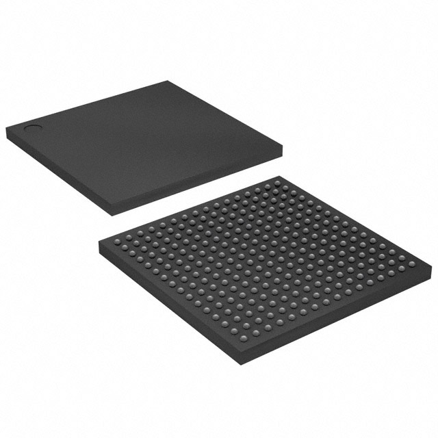
Spartan®-II Field Programmable Gate Array (FPGA) IC 176 40960 2700 256-BGA |
|---|---|
| Quantity | 183 Available (as of June 18, 2026) |
| Product Category | Field Programmable Gate Array (FPGA) |
|---|---|
| Manufacturer | AMD |
| Manufacturing Status | Last Time Buy |
| Manufacturer Standard Lead Time | 12 Weeks |
| Datasheet |
Specifications & Environmental
| Device Package | 256-FBGA (17x17) | Grade | Commercial | Operating Temperature | 0°C – 85°C | ||
|---|---|---|---|---|---|---|---|
| Package / Case | 256-BGA | Number of I/O | 176 | Voltage | 2.375 V - 2.625 V | ||
| Mounting Method | Surface Mount | RoHS Compliance | ROHS3 Compliant | REACH Compliance | REACH Unaffected | ||
| Moisture Sensitivity Level | 3 (168 Hours) | Number of LABs/CLBs | 600 | Number of Logic Elements/Cells | 2700 | ||
| Number of Gates | 100000 | ECCN | EAR99 | HTS Code | 8542.39.0001 | ||
| Qualification | N/A | Total RAM Bits | 40960 |
Overview of XC2S100-5FGG256C – Spartan®-II Field Programmable Gate Array (FPGA) IC 176 40960 2700 256-BGA
The XC2S100-5FGG256C is a Spartan®-II family FPGA from AMD presented in a 256-ball BGA package. It delivers a mid-range programmable logic resource set suitable for commercial embedded designs that require moderate gate count, on-chip memory, and a substantial number of I/O pins.
Built for surface-mount assembly and standard commercial operating temperatures, this device balances integration and configurability with straightforward power requirements to support a variety of digital logic implementations.
Key Features
- Core Architecture Spartan®-II FPGA architecture in a field-programmable device designed for custom digital logic implementation.
- Logic Capacity Approximately 2,700 logic elements representing roughly 100,000 gates for implementing custom combinational and sequential logic functions.
- Embedded Memory Approximately 0.04 Mbits of on-chip RAM (40,960 bits) to support buffering, small data stores, and state machines.
- I/O Density 176 user I/O pins suitable for interfacing with multiple peripherals, buses, and external devices.
- Power Single-core supply requirement in the range 2.375 V–2.625 V for core power planning.
- Package & Mounting 256-BGA, supplied as 256-FBGA (17×17), surface-mount package to support compact PCB layouts and higher routing density.
- Operating Range Commercial grade with an operating temperature span of 0 °C–85 °C.
- Regulatory RoHS compliant for adherence to common lead-free manufacturing requirements.
Typical Applications
- Custom digital logic implementations Use the device to realize bespoke finite state machines, glue logic, and moderate-complexity datapaths within the 100,000-gate capability.
- I/O-heavy interface control Leverage 176 I/O pins to handle multi-signal interfaces, parallel buses, and multiple peripheral connections in commercial systems.
- Embedded buffering and control Employ the on-chip RAM (40,960 bits) for small buffering tasks, lookup tables, and local state storage in control applications.
- Compact, surface-mounted designs The 256-FBGA (17×17) package supports high-density PCB integration where board space and routing are constrained.
Unique Advantages
- Balanced logic and gate density: ~2,700 logic elements and ~100,000 gates provide a middle-ground resource set for many commercial designs without overspecifying capacity.
- Generous I/O count: 176 I/O pins allow direct interfacing to multiple peripherals and buses, reducing the need for external I/O expanders.
- On-chip memory availability: Approximately 0.04 Mbits of embedded RAM supports local buffering and small data structures, simplifying board-level memory requirements.
- Compact package for tight PCBs: 256-FBGA (17×17) surface-mount construction enables dense routing and a reduced PCB footprint.
- Commercial temperature and RoHS compliance: Specified 0 °C–85 °C operating range and RoHS compliance help align the device with standard commercial manufacturing and deployment environments.
Why Choose XC2S100-5FGG256C?
The XC2S100-5FGG256C positions itself as a practical choice for engineers needing a commercially graded, mid-range FPGA that combines usable logic capacity, on-chip memory, and a high I/O count in a compact BGA package. Its voltage and temperature specifications simplify power and thermal planning for typical commercial embedded systems.
This device is well suited for design teams implementing custom logic, interface controllers, or compact board-level solutions where a balance of gates, I/O, and package density provides long-term value across multiple product iterations.
If you would like pricing, availability, or to request a quote for the XC2S100-5FGG256C, submit a quote request or contact sales to start the procurement process.


Date Founded: 1969
Headquarters: Santa Clara, California, USA
Employees: 25,000+
Revenue: $22.68 Billion
Certifications and Memberships: ISO9001:2015, RoHS, REACH


