
XC4VLX80-10FF1148C
| Part Description |
Virtex®-4 LX Field Programmable Gate Array (FPGA) IC 768 3686400 80640 1148-BBGA, FCBGA |
|---|---|
| Quantity | 405 Available (as of June 18, 2026) |

| Product Category | Field Programmable Gate Array (FPGA) |
|---|---|
| Manufacturer | AMD |
| Manufacturing Status | Active |
| Manufacturer Standard Lead Time | 25 Weeks |
| Datasheet |
Specifications & Environmental
| Device Package | 1148-FCPBGA (35x35) | Grade | Commercial | Operating Temperature | 0°C – 85°C | ||
|---|---|---|---|---|---|---|---|
| Package / Case | 1148-BBGA, FCBGA | Number of I/O | 768 | Voltage | 1.14 V - 1.26 V | ||
| Mounting Method | Surface Mount | RoHS Compliance | RoHS non-compliant | REACH Compliance | REACH Unaffected | ||
| Moisture Sensitivity Level | 4 (72 Hours) | Number of LABs/CLBs | 8960 | Number of Logic Elements/Cells | 80640 | ||
| Number of Gates | N/A | ECCN | 3A001A7A | HTS Code | 8542.39.0001 | ||
| Qualification | N/A | Total RAM Bits | 3686400 |
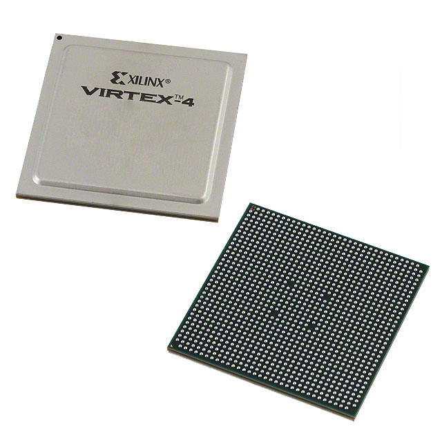
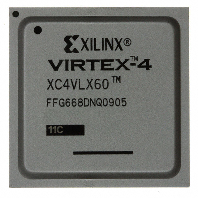
Overview of XC4VLX80-10FF1148C – Virtex®-4 LX Field Programmable Gate Array (FPGA) IC 768 3686400 80640 1148-BBGA, FCBGA
The XC4VLX80-10FF1148C is a Virtex®-4 LX Field Programmable Gate Array (FPGA) from AMD. It provides a high-density programmable fabric with 80,640 logic elements and 8,960 configurable logic blocks (CLBs), combined with on-chip RAM for embedded buffering and state storage.
Designed for systems that require large I/O counts and significant programmable logic capacity, this surface-mount FCBGA device offers a compact 1148-ball package and a defined commercial operating range for reliable deployment in standard-temperature electronic applications.
Key Features
- Programmable Logic Capacity — 80,640 logic elements and 8,960 configurable logic blocks (CLBs) provide substantial resources for implementing complex logic, control, and datapath functions.
- Embedded Memory — Approximately 3.69 Mbits of on-chip RAM enable local buffering, state storage, and small data structures without external memory.
- High I/O Count — 768 user I/O pins support extensive peripheral interfacing and multi-channel connectivity within a single device.
- Package & Mounting — 1148-ball FCBGA (1148-FCPBGA, 35×35) surface-mount package balances high pin count with a compact footprint for board-level integration.
- Power Supply — Core voltage support from 1.14 V to 1.26 V allows straightforward power design within the specified range.
- Operating Grade & Temperature — Commercial grade device with an operating temperature range of 0 °C to 85 °C suitable for standard commercial applications.
- Regulatory Compliance — RoHS compliant, supporting environmentally conscious designs.
Typical Applications
- High-density logic integration — Use the large logic element and CLB counts to consolidate multiple digital functions into a single FPGA, reducing board-level component count.
- I/O-rich interfacing — Leverage 768 I/O pins for multi-channel signal aggregation, custom peripheral interfaces, or dense connector routing.
- On-chip buffering and state machines — Approximately 3.69 Mbits of embedded RAM supports local data buffering, FIFOs, and finite-state implementations without immediate need for external memory.
- Compact board-level designs — The 1148-ball FCBGA package enables high pin density in a compact footprint for space-constrained PCB layouts.
Unique Advantages
- Substantial programmable capacity: 80,640 logic elements and 8,960 CLBs provide headroom for complex logic designs and integration of multiple subsystems on one device.
- Large I/O budget: 768 I/O pins simplify multi-interface designs and reduce the need for external multiplexing or I/O expanders.
- Embedded memory for local data handling: Approximately 3.69 Mbits of on-chip RAM reduces latency and external memory dependency for buffering and state storage.
- Compact, high-density package: The 1148-ball FCBGA (35 × 35) enables a balance of pin count and PCB area efficiency for dense system designs.
- Environmental compliance: RoHS compliance helps meet regulatory requirements for lead-free designs.
- Defined power and thermal envelope: Clear core voltage range (1.14–1.26 V) and commercial temperature rating support reliable integration into standard commercial electronics.
Why Choose XC4VLX80-10FF1148C?
The XC4VLX80-10FF1148C positions itself as a high-capacity Virtex-4 LX FPGA option for designs that need extensive programmable logic, abundant I/O, and on-chip memory in a compact FCBGA package. Its combination of 80,640 logic elements, 8,960 CLBs, and approximately 3.69 Mbits of embedded RAM enables consolidation of complex digital functions while supporting dense external interfacing.
This commercial-grade device is suitable for teams and designs targeting standard-temperature electronics that require a RoHS-compliant, high-density FPGA with clear power and package specifications. It delivers long-term design value through integration potential and a well-defined hardware footprint for board-level planning.
Request a quote or submit a purchase inquiry to receive pricing and availability information for the XC4VLX80-10FF1148C. Our team can provide lead-time details and order support to help move your design forward.


Date Founded: 1969
Headquarters: Santa Clara, California, USA
Employees: 25,000+
Revenue: $22.68 Billion
Certifications and Memberships: ISO9001:2015, RoHS, REACH


