
XC5202-6PC84C
| Part Description |
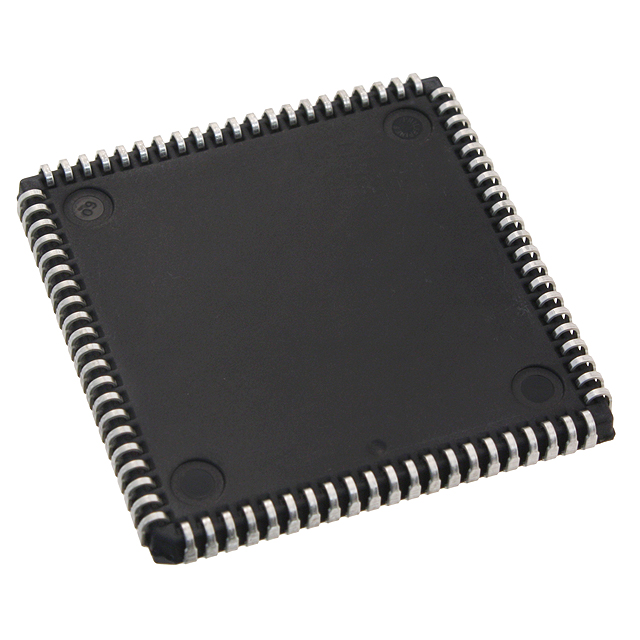
XC5200 Field Programmable Gate Array (FPGA) IC 65 256 84-LCC (J-Lead) |
|---|---|
| Quantity | 921 Available (as of June 10, 2026) |
| Product Category | Field Programmable Gate Array (FPGA) |
|---|---|
| Manufacturer | AMD |
| Manufacturing Status | Obsolete |
| Manufacturer Standard Lead Time | Contact Us |
| Datasheet |
Specifications & Environmental
| Device Package | 84-PLCC (29.31x29.31) | Grade | Commercial | Operating Temperature | 0°C – 85°C | ||
|---|---|---|---|---|---|---|---|
| Package / Case | 84-LCC (J-Lead) | Number of I/O | 65 | Voltage | 4.75 V - 5.25 V | ||
| Mounting Method | Surface Mount | RoHS Compliance | RoHS non-compliant | REACH Compliance | REACH Unaffected | ||
| Moisture Sensitivity Level | 3 (168 Hours) | Number of LABs/CLBs | 64 | Number of Logic Elements/Cells | 256 | ||
| Number of Gates | 3000 | ECCN | EAR99 | HTS Code | 8542.39.0001 | ||
| Qualification | N/A |
Overview of XC5202-6PC84C – Field Programmable Gate Array (FPGA) IC, 65 I/O, 256 Logic Elements, 84‑LCC (J‑Lead)
The XC5202-6PC84C is a commercial-grade Field Programmable Gate Array (FPGA) offered in an 84‑lead LCC (J‑Lead) surface-mount package. It provides a compact, reprogrammable digital fabric with 256 logic elements and up to 65 I/O pins, suitable for small to medium complexity control and interfacing tasks.
With a 5 V supply range (4.75 V to 5.25 V), approximately 3,000 equivalent gates and a commercial operating range of 0 °C to 85 °C, this device targets designs that require flexible logic implementation in a compact PLCC footprint (84‑PLCC, 29.31 × 29.31 mm).
Key Features
- Core Logic Capacity — 256 logic elements providing the programmable building blocks for combinational and sequential logic implementation.
- IO Resources — 65 user-accessible I/O pins to support a variety of peripheral interfaces and system glue logic.
- Gate Equivalent — Approximately 3,000 gates of usable logic capacity for implementing control, decoding, and interface functions.
- Power — Single 5 V supply compatible with 4.75 V to 5.25 V systems for straightforward integration into legacy 5 V designs.
- Package & Mounting — Surface-mount 84‑lead LCC (J‑Lead) package; supplier device package listed as 84‑PLCC (29.31 × 29.31 mm) for compact board-level integration.
- Operating Range & Grade — Commercial operating temperature range of 0 °C to 85 °C; commercial grade device suitable for consumer and industrial-adjacent applications.
- Regulatory Compliance — RoHS compliant to meet common environmental and manufacturing requirements.
Typical Applications
- Control Logic and Glue Functions — Implement custom state machines and interface glue between processors, sensors, and peripherals using the device's logic elements and 65 I/O pins.
- Peripheral Interface and Bus Bridging — Use available I/O and programmable logic to adapt or bridge legacy 5 V buses and mixed-voltage modules.
- User Interface and Simple Timing — Implement LED drivers, button scanning, debouncing, and simple timing/sequencing tasks within the device's logic capacity.
- Prototyping and Small-Scale FPGA Integration — Deploy in early-stage designs that require reprogrammability and compact PLCC packaging for evaluation or low-volume production.
Unique Advantages
- Compact Programmable Solution: Delivers 256 logic elements and 65 I/O in an 84‑lead PLCC package, minimizing board space while retaining flexible reprogrammability.
- 5 V System Compatibility: Operates from 4.75 V to 5.25 V, simplifying integration into existing 5 V designs and reducing the need for level-shifting in many applications.
- RoHS Compliance: Environmentally compliant manufacturing reduces supply-chain complexity for assemblies requiring RoHS components.
- Surface-Mount Package: J‑lead LCC surface-mount form factor supports automated assembly and consistent board-level placement.
- Predictable Commercial Performance: Rated for 0 °C to 85 °C, providing defined operating boundaries for consumer and commercial electronics projects.
Why Choose XC5202-6PC84C?
The XC5202-6PC84C positions itself as a compact, reprogrammable FPGA for designers who need straightforward digital logic integration in a 5 V environment. Its combination of 256 logic elements, roughly 3,000 gate-equivalents, and 65 I/O pins makes it well suited to control, interfacing, and modest sequencing tasks where board space and reprogrammability are priorities.
This device is appropriate for teams developing consumer and commercial electronics that benefit from configurable logic in a PLCC package, offering RoHS compliance and surface-mount assembly compatibility for streamlined production and procurement.
Request a quote or submit a parts inquiry to receive pricing and availability for the XC5202-6PC84C.


Date Founded: 1969
Headquarters: Santa Clara, California, USA
Employees: 25,000+
Revenue: $22.68 Billion
Certifications and Memberships: ISO9001:2015, RoHS, REACH


