
XC5VLX110-1FFG1760CES
| Part Description |
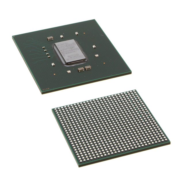
Virtex®-5 LX Field Programmable Gate Array (FPGA) IC 800 4718592 110592 1760-BBGA, FCBGA |
|---|---|
| Quantity | 254 Available (as of June 15, 2026) |

| Product Category | Field Programmable Gate Array (FPGA) |
|---|---|
| Manufacturer | AMD |
| Manufacturing Status | Obsolete |
| Manufacturer Standard Lead Time | Contact Us |
| Datasheet |
Specifications & Environmental
| Device Package | 1760-FCBGA (42.5x42.5) | Grade | Commercial | Operating Temperature | 0°C – 85°C | ||
|---|---|---|---|---|---|---|---|
| Package / Case | 1760-BBGA, FCBGA | Number of I/O | 800 | Voltage | 950 mV - 1.05 V | ||
| Mounting Method | Surface Mount | RoHS Compliance | Unknown | REACH Compliance | REACH Unaffected | ||
| Moisture Sensitivity Level | 4 (72 Hours) | Number of LABs/CLBs | 8640 | Number of Logic Elements/Cells | 110592 | ||
| Number of Gates | N/A | ECCN | 3A001A7A | HTS Code | 8542.39.0001 | ||
| Qualification | N/A | Total RAM Bits | 4718592 |
Overview of XC5VLX110-1FFG1760CES – Virtex®-5 LX Field Programmable Gate Array (FPGA) IC
The XC5VLX110-1FFG1760CES is a Virtex®-5 LX field programmable gate array manufactured by AMD, supplied in a 1760-ball FCBGA package (42.5 × 42.5 mm). It provides a high-density programmable fabric with 110,592 logic elements and approximately 4.72 Mbits of embedded memory to support complex digital designs with extensive I/O.
Designed for surface-mount board-level integration, this commercial-grade device supports up to 800 I/O pins and operates from a core voltage range of 0.95 V to 1.05 V with an ambient operating temperature range of 0 °C to 85 °C. The part is RoHS compliant.
Key Features
- Core Logic 110,592 logic elements (cells) provide a large programmable fabric for implementing complex state machines, datapaths and custom logic functions.
- Embedded Memory Approximately 4.72 Mbits of on-chip RAM to store buffers, FIFOs, lookup tables and other data structures without external memory.
- I/O Capacity Up to 800 I/O pins enable wide parallel interfaces, dense connectivity to peripherals, sensors and external devices.
- Power Core supply voltage range of 0.95 V to 1.05 V for integration with regulated power delivery designs.
- Package and Mounting 1760-FCBGA package (42.5 × 42.5 mm) in a surface-mount form factor suitable for compact, high-density PCB layouts.
- Temperature and Grade Commercial grade operation from 0 °C to 85 °C for standard commercial and industrial environment deployments.
- Environmental Compliance RoHS compliant to support lead-free manufacturing processes.
Typical Applications
- High-density digital processing — Leverage 110,592 logic elements and on-chip RAM for custom datapaths, signal processing blocks and parallel compute tasks.
- Interface aggregation — Use up to 800 I/O pins to consolidate multiple sensor, peripheral or bus interfaces into a single programmable device.
- Prototyping and system validation — The combination of large logic capacity and embedded memory makes the device suitable for hardware prototyping of complex digital systems.
- Embedded control and glue logic — Implement control engines, protocol bridges and timing-critical logic using the device’s programmable fabric and plentiful I/O.
Unique Advantages
- Large programmable capacity: 110,592 logic elements enable implementation of complex designs without partitioning across multiple devices.
- Substantial on-chip memory: Approximately 4.72 Mbits of embedded RAM reduce dependency on external memory components and simplify board design.
- Extensive connectivity: Up to 800 I/Os support high pin-count interfaces and parallel signal routing for demanding system architectures.
- Surface-mount FCBGA packaging: 1760-ball FCBGA (42.5 × 42.5 mm) balances high I/O density with a compact footprint for modern PCBs.
- Commercial temperature range: Rated for 0 °C to 85 °C operation to meet standard commercial application requirements.
- RoHS compliant: Supports lead-free manufacturing and environmental compliance requirements.
Why Choose XC5VLX110-1FFG1760CES?
The XC5VLX110-1FFG1760CES positions itself as a high-capacity Virtex®-5 LX FPGA option for engineers needing substantial logic resources, embedded memory and large I/O counts in a surface-mount FCBGA package. Its combination of 110,592 logic elements, approximately 4.72 Mbits of on-chip RAM and up to 800 I/O pins makes it suitable for complex digital designs, interface consolidation and hardware prototyping under commercial temperature conditions.
This AMD-manufactured device offers designers a scalable programmable platform that simplifies BOM and board complexity by integrating logic, memory and extensive I/O. Its RoHS compliance and defined electrical and thermal operating ranges help support reproducible production and long-term deployment in commercial products.
Request a quote or submit an inquiry to receive pricing, availability and technical support for XC5VLX110-1FFG1760CES.


Date Founded: 1969
Headquarters: Santa Clara, California, USA
Employees: 25,000+
Revenue: $22.68 Billion
Certifications and Memberships: ISO9001:2015, RoHS, REACH


