
XC5VLX50T-1FFG1136C
| Part Description |
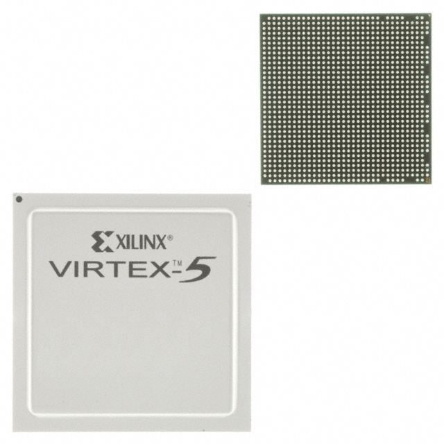
Virtex®-5 LXT Field Programmable Gate Array (FPGA) IC 480 2211840 46080 1136-BBGA, FCBGA |
|---|---|
| Quantity | 688 Available (as of June 15, 2026) |

| Product Category | Field Programmable Gate Array (FPGA) |
|---|---|
| Manufacturer | AMD |
| Manufacturing Status | Active |
| Manufacturer Standard Lead Time | 12 Weeks |
| Datasheet |
Specifications & Environmental
| Device Package | 1136-FCBGA (35x35) | Grade | Commercial | Operating Temperature | 0°C – 85°C | ||
|---|---|---|---|---|---|---|---|
| Package / Case | 1136-BBGA, FCBGA | Number of I/O | 480 | Voltage | 950 mV - 1.05 V | ||
| Mounting Method | Surface Mount | RoHS Compliance | ROHS3 Compliant | REACH Compliance | REACH Unaffected | ||
| Moisture Sensitivity Level | 4 (72 Hours) | Number of LABs/CLBs | 3600 | Number of Logic Elements/Cells | 46080 | ||
| Number of Gates | N/A | ECCN | 3A001A7A | HTS Code | 8542.39.0001 | ||
| Qualification | N/A | Total RAM Bits | 2211840 |
Overview of XC5VLX50T-1FFG1136C – Virtex®-5 LXT Field Programmable Gate Array (FPGA)
The XC5VLX50T-1FFG1136C is a Virtex-5 LXT field programmable gate array (FPGA) IC from AMD, offered in a 1136-BBGA FCBGA package. It targets designs that require substantial on-chip logic, embedded memory and a high count of I/O signals within a commercial-grade operating range.
Key architectural resources include 46,080 logic elements, approximately 2.21 Mbits of embedded RAM, 480 I/O, and 3,600 configurable logic blocks (CLBs), making the device suitable for logic- and I/O-dense implementations while operating from a 950 mV to 1.05 V core supply.
Key Features
- Core / Logic Configurable Logic Blocks (CLBs): 3,600 and 46,080 logic elements provide the device's primary programmable resources for implementing complex logic functions.
- Embedded Memory Approximately 2.21 Mbits of on-chip RAM to support buffering, FIFOs and intermediate data storage without requiring external memory for many common functions.
- I/O Capacity 480 general-purpose I/O pins to support multiple interfaces and parallel connectivity within a single device.
- Power Core voltage supply range of 950 mV to 1.05 V for the FPGA core.
- Package & Mounting 1136-BBGA, FCBGA package (supplier device package: 1136-FCBGA (35x35)), designed for surface-mount PCB assembly.
- Operating Range & Grade Commercial grade with an operating temperature range of 0°C to 85°C.
- Environmental Compliance RoHS compliant.
Typical Applications
- High-density logic implementations Use the device's 46,080 logic elements and 3,600 CLBs to implement complex programmable logic and custom processing pipelines.
- Memory-centric functions Approximately 2.21 Mbits of embedded RAM support data buffering, FIFO structures and intermediate storage within the FPGA fabric.
- I/O-intensive systems Up to 480 I/O enable multi-protocol interfacing, parallel bus implementations and aggregation of signals without additional interface chips.
- Compact, board-level integration The 1136-FCBGA surface-mount package supports dense PCB layouts where board area and integration are critical.
Unique Advantages
- Substantial programmable logic: 46,080 logic elements and 3,600 CLBs allow integration of complex logic and control functions that reduce external components.
- On-chip memory reduces external BOM: Approximately 2.21 Mbits of embedded RAM can lower the need for external memory devices in many designs.
- Large I/O footprint: 480 I/O simplifies multi-interface designs and minimizes the need for external multiplexing or expanders.
- Compact FCBGA package: The 1136-FCBGA (35x35) package supports high-density board designs while maintaining surface-mount assembly compatibility.
- Commercial operating range: 0°C to 85°C and RoHS compliance align the device with mainstream commercial product requirements.
- Low-voltage core operation: Core supply range of 950 mV to 1.05 V fits modern low-voltage power architectures.
Why Choose XC5VLX50T-1FFG1136C?
The XC5VLX50T-1FFG1136C positions itself as a commercial-grade Virtex-5 LXT FPGA with a balanced mix of logic capacity, embedded memory and I/O resources in a compact FCBGA package. It is appropriate for engineers and procurement teams specifying a surface-mount FPGA that consolidates logic, buffering and interface requirements on a single device.
For designs that demand substantial on-chip programmable resources and extensive I/O, this part offers a clear specification set—46,080 logic elements, approximately 2.21 Mbits of on-chip RAM, 480 I/O—backed by AMD manufacturing and RoHS compliance for mainstream electronic products.
Request a quote to confirm availability and pricing for the XC5VLX50T-1FFG1136C and to discuss volume and lead-time options.


Date Founded: 1969
Headquarters: Santa Clara, California, USA
Employees: 25,000+
Revenue: $22.68 Billion
Certifications and Memberships: ISO9001:2015, RoHS, REACH


