
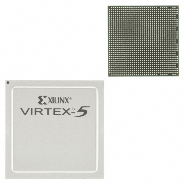
XC5VLX85T-2FFG1136C
| Part Description |
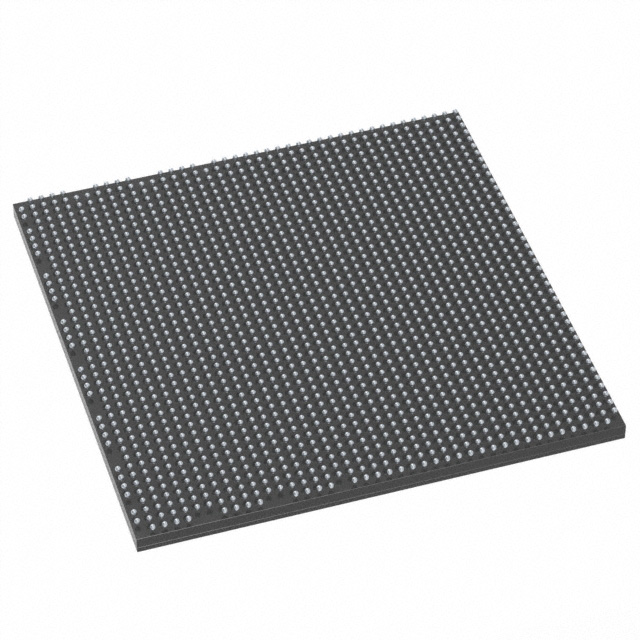
Virtex®-5 LXT Field Programmable Gate Array (FPGA) IC 480 3981312 82944 1136-BBGA, FCBGA |
|---|---|
| Quantity | 1,603 Available (as of June 14, 2026) |

| Product Category | Field Programmable Gate Array (FPGA) |
|---|---|
| Manufacturer | AMD |
| Manufacturing Status | Active |
| Manufacturer Standard Lead Time | 12 Weeks |
| Datasheet |
Specifications & Environmental
| Device Package | 1136-FCBGA (35x35) | Grade | Commercial | Operating Temperature | 0°C – 85°C | ||
|---|---|---|---|---|---|---|---|
| Package / Case | 1136-BBGA, FCBGA | Number of I/O | 480 | Voltage | 950 mV - 1.05 V | ||
| Mounting Method | Surface Mount | RoHS Compliance | ROHS3 Compliant | REACH Compliance | REACH Unaffected | ||
| Moisture Sensitivity Level | 4 (72 Hours) | Number of LABs/CLBs | 6480 | Number of Logic Elements/Cells | 82944 | ||
| Number of Gates | N/A | ECCN | 3A001A7A | HTS Code | 8542.39.0001 | ||
| Qualification | N/A | Total RAM Bits | 3981312 |
Overview of XC5VLX85T-2FFG1136C – Virtex®-5 LXT FPGA, 1136‑FCBGA
The XC5VLX85T-2FFG1136C is a Virtex®-5 LXT field programmable gate array (FPGA) from AMD designed for commercial applications that require high logic density, abundant I/O and on-chip memory. It combines 6,480 CLBs and 82,944 logic elements with substantial embedded RAM and a large I/O count to support complex digital designs.
Packaged in a 1136‑FCBGA (35×35) surface-mount package and specified for commercial operation (0 °C to 85 °C), this device is suitable for designs that need compact, high-capacity programmable logic with tightly specified core voltage requirements.
Key Features
- Core Logic 6,480 CLBs delivering 82,944 logic elements for implementing large-scale digital logic and custom datapaths.
- Embedded Memory Approximately 3.98 Mbits of on-chip RAM (3,981,312 total RAM bits) to support buffering, FIFOs and local storage.
- I/O Capacity 480 I/O pins to interface with high-pin-count peripherals, memory, or multi-lane communications links.
- Power Supply Core voltage specified from 0.95 V to 1.05 V, enabling designs that target this specific core power envelope.
- Package & Mounting 1136‑BBGA / 1136‑FCBGA package, supplier device package 1136‑FCBGA (35×35); surface-mount mounting for board-level integration.
- Operating Range & Grade Commercial grade device rated for 0 °C to 85 °C operation.
- Environmental Compliance RoHS compliant.
Typical Applications
- High-density digital processing Implement complex custom logic, signal processing pipelines or multi-module controllers using the device’s large CLB and logic element count.
- Communications and interfaces Support for designs requiring many I/O connections makes this device suitable for protocol bridging, aggregation or multi-channel interfaces.
- Embedded systems and control Use the on-chip RAM and high logic capacity for embedded controllers, real-time processing and hardware-accelerated tasks in commercial products.
- Prototype and system integration Dense logic and plentiful I/O enable rapid prototyping of complex systems and consolidation of multiple functions into a single FPGA.
Unique Advantages
- High logic capacity: 82,944 logic elements provide the headroom to implement large, integrated designs without partitioning across multiple devices.
- Substantial embedded memory: Approximately 3.98 Mbits of on-chip RAM reduces external memory dependence for buffering and local storage.
- Large I/O count: 480 I/Os simplify board-level routing and enable direct connections to many peripherals or multi-lane interfaces.
- Compact, high-density package: 1136‑FCBGA (35×35) delivers high pin density in a surface-mount form factor for space-constrained PCBs.
- Commercial temperature rating: Specified 0 °C to 85 °C operation aligns with standard commercial product deployments.
- RoHS compliant: Meets environmental compliance requirements for lead-free production environments.
Why Choose XC5VLX85T-2FFG1136C?
The XC5VLX85T-2FFG1136C positions itself as a high-capacity, commercial-grade FPGA option for engineers who need extensive logic resources, significant embedded RAM and a large number of I/Os in a single package. With a defined core voltage window and a surface-mount 1136‑FCBGA package, this device is suitable for compact, integrated designs where consolidation and board-level density matter.
Its combination of CLBs, logic elements, on-chip memory and I/O makes it a practical choice for teams developing advanced digital processing, communications interfaces or embedded control systems that require a reliable, high-density programmable platform.
Request a quote or submit an inquiry to get pricing, availability and additional technical details for the XC5VLX85T-2FFG1136C.


Date Founded: 1969
Headquarters: Santa Clara, California, USA
Employees: 25,000+
Revenue: $22.68 Billion
Certifications and Memberships: ISO9001:2015, RoHS, REACH


