
XC7V585T-3FFG1761E
| Part Description |
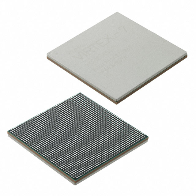
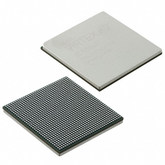
Virtex®-7 T Field Programmable Gate Array (FPGA) IC 850 29306880 582720 1760-BBGA, FCBGA |
|---|---|
| Quantity | 834 Available (as of June 10, 2026) |

| Product Category | Field Programmable Gate Array (FPGA) |
|---|---|
| Manufacturer | AMD |
| Manufacturing Status | Active |
| Manufacturer Standard Lead Time | 16 Weeks |
| Datasheet |
Specifications & Environmental
| Device Package | 1761-FCBGA (42.5x42.5) | Grade | Extended | Operating Temperature | 0°C – 100°C | ||
|---|---|---|---|---|---|---|---|
| Package / Case | 1760-BBGA, FCBGA | Number of I/O | 850 | Voltage | 970 mV - 1.03 V | ||
| Mounting Method | Surface Mount | RoHS Compliance | ROHS3 Compliant | REACH Compliance | REACH Unaffected | ||
| Moisture Sensitivity Level | 4 (72 Hours) | Number of LABs/CLBs | 45525 | Number of Logic Elements/Cells | 582720 | ||
| Number of Gates | N/A | ECCN | 3A001A7A | HTS Code | 8542.39.0001 | ||
| Qualification | N/A | Total RAM Bits | 29306880 |
Overview of XC7V585T-3FFG1761E – Virtex®-7 T Field Programmable Gate Array (FPGA)
The XC7V585T-3FFG1761E is a Virtex®-7 T Field Programmable Gate Array in a 1760-BBGA FCBGA package designed for high-density, reconfigurable logic implementations. It provides a large on-chip resource set including 582,720 logic elements, approximately 29.3 Mbits of embedded memory, and 850 I/O to address complex system integration and custom hardware functions.
Built for surface-mount assembly and specified for an operating temperature range of 0 °C to 100 °C with an extended grade, this device suits applications that require significant logic capacity, abundant I/O, and a compact 42.5 mm × 42.5 mm FCBGA package footprint. The device supply range is specified from 970 mV to 1.03 V and it is RoHS compliant.
Key Features
- Core Capacity 582,720 logic elements provide extensive programmable fabric for large-scale custom logic, parallel datapaths, and complex finite-state implementations.
- Embedded Memory Approximately 29.3 Mbits of on-chip RAM for buffering, packet storage, and algorithm working memory directly inside the FPGA fabric.
- I/O Density 850 I/O pins enable wide parallel interfaces, multi-channel connectivity, and flexible board-level interfacing options.
- Power Supply Core supply specified from 970 mV to 1.03 V to match board power design and regulator selection requirements.
- Package and Mounting 1760-BBGA (supplier device package 1761-FCBGA, 42.5 × 42.5 mm) in a surface-mount FCBGA format for high-density system assemblies.
- Operating Range and Grade Extended-grade device specified for operation from 0 °C to 100 °C, supporting designs with elevated ambient requirements within that range.
- Compliance RoHS compliant to support lead-free assembly processes and regulatory requirements.
Typical Applications
- Custom Hardware Acceleration Large logic capacity and significant embedded memory enable implementation of application-specific accelerators and parallel processing engines.
- High-Density I/O Systems 850 I/O pins make the device suitable for designs that require extensive external interfacing, multi-lane data capture, or large sensor arrays.
- Complex Digital Prototyping The combination of logic elements and on-chip RAM supports full-system prototyping and emulation of complex digital designs.
Unique Advantages
- Extensive Logic Resources: 582,720 logic elements provide headroom for large, multi-module FPGA designs without immediately needing an external ASIC.
- Substantial On-Chip Memory: Approximately 29.3 Mbits of embedded RAM reduces dependence on external memory for many buffering and local storage tasks.
- High I/O Count: 850 I/O pins simplify integration with multi-channel interfaces and parallel data paths, reducing external multiplexing or bridge logic.
- Compact FCBGA Packaging: 1760-BBGA (42.5 × 42.5 mm) package lets designers place a high-capacity FPGA in compact PCB layouts while supporting surface-mount assembly.
- Design-Ready Supply Range: 970 mV to 1.03 V supply specification allows precise power budgeting and regulator selection for board-level power design.
- Regulatory Compliance: RoHS compliance supports lead-free manufacturing and regulatory adherence.
Why Choose XC7V585T-3FFG1761E?
The XC7V585T-3FFG1761E positions itself as a high-capacity, reconfigurable solution for designs that require extensive programmable logic, ample embedded memory, and a large number of I/O signals within a compact FCBGA package. Its extended-grade specification and defined supply range help align system-level thermal and power planning for production deployments operating within 0 °C to 100 °C.
This device is well suited for engineering teams building complex accelerators, high-channel-count interfaces, or full-platform prototypes that benefit from significant on-chip resources and a single-package integration strategy. Its resource balance supports scalability and long-term design evolution within the Virtex®-7 T family context.
Request a quote or submit a purchase inquiry today to obtain pricing, availability, and ordering information for the XC7V585T-3FFG1761E.


Date Founded: 1969
Headquarters: Santa Clara, California, USA
Employees: 25,000+
Revenue: $22.68 Billion
Certifications and Memberships: ISO9001:2015, RoHS, REACH


