
XCV150-5BG352C
| Part Description |
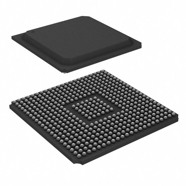
Virtex® Field Programmable Gate Array (FPGA) IC 260 49152 3888 352-LBGA Exposed Pad, Metal |
|---|---|
| Quantity | 1,004 Available (as of June 15, 2026) |

| Product Category | Field Programmable Gate Array (FPGA) |
|---|---|
| Manufacturer | AMD |
| Manufacturing Status | Obsolete |
| Manufacturer Standard Lead Time | Contact Us |
| Datasheet |
Specifications & Environmental
| Device Package | 352-MBGA (35x35) | Grade | Commercial | Operating Temperature | 0°C – 85°C | ||
|---|---|---|---|---|---|---|---|
| Package / Case | 352-LBGA Exposed Pad, Metal | Number of I/O | 260 | Voltage | 2.375 V - 2.625 V | ||
| Mounting Method | Surface Mount | RoHS Compliance | RoHS non-compliant | REACH Compliance | REACH Unaffected | ||
| Moisture Sensitivity Level | 3 (168 Hours) | Number of LABs/CLBs | 864 | Number of Logic Elements/Cells | 3888 | ||
| Number of Gates | 164674 | ECCN | 3A991D | HTS Code | 8542.39.0001 | ||
| Qualification | N/A | Total RAM Bits | 49152 |
Overview of XCV150-5BG352C – Virtex® FPGA, 3,888 logic elements; 49,152-bit RAM; 260 I/O; 352-LBGA
The XCV150-5BG352C is an SRAM-based Virtex® Field Programmable Gate Array offering 3,888 logic elements and 49,152 bits of on-chip block RAM in a 352-LBGA exposed-pad metal package. It is designed for applications that require high-density programmable logic, flexible I/O, and on-chip memory in a compact surface-mount footprint.
Part of the Virtex family, this device provides advanced clock-management and hierarchical memory resources, plus multi-standard I/O support and in-system re-programmability for rapid development and iterative design refinement.
Key Features
- Logic Capacity — 3,888 logic elements supporting a total of 164,674 system gates, enabling complex logic implementation within a single device.
- On-Chip Memory — 49,152 bits of embedded block RAM with configurable LUT-based RAM options and support for dual-ported and shift-register configurations.
- I/O Resources — 260 user I/O pins and multi-standard SelectIO™ interfaces providing broad interface flexibility and direct connectivity options.
- Clock Management — Built-in clock circuitry with four dedicated delay-locked loops (DLLs), four primary low-skew global clock nets, and 24 secondary local clock nets for advanced clock control.
- Configuration & Development — SRAM-based in-system configuration with unlimited re-programmability and multiple programming modes for iterative design and field updates.
- Package & Mounting — 352-LBGA exposed pad, metal package (supplier package: 352-MBGA 35×35) for surface-mount assembly.
- Power & Operating Range — Core supply range 2.375 V to 2.625 V; commercial operating temperature 0 °C to 85 °C.
- Manufacturing & Compliance — 100% factory tested and RoHS compliant.
Typical Applications
- High-performance system logic — Implement custom datapaths, control logic, and protocol engines using the device’s dense logic and embedded RAM.
- Memory interface and buffering — Use on-chip RAM and fast external-memory interfaces for buffering, packet handling, and intermediate storage.
- PCI/Compact PCI systems — Series-level support includes 66‑MHz PCI compliance and hot-swappable Compact PCI capability for modular system designs.
- Clocked digital subsystems — Advanced clock-management resources enable precise clock distribution for synchronous designs and multi-clock domains.
Unique Advantages
- High-density programmable logic: 3,888 logic elements and 164,674 system gates let you consolidate complex functions into a single FPGA, reducing board-level components.
- Flexible on-chip memory: 49,152 bits of block RAM and LUT-configurable RAM modes simplify data buffering and state storage without external memory in many designs.
- Versatile I/O: 260 I/O pins with multi-standard SelectIO support give designers broad interface options for diverse peripherals and external devices.
- Integrated clock control: Four DLLs and multi-level clock distribution provide deterministic timing and simplify timing closure across large designs.
- Compact, assembly-ready package: 352-LBGA exposed-pad metal package supports surface-mount manufacturing and thermal considerations in space-constrained layouts.
- Development ecosystem support: Family-level support by established development systems facilitates design, simulation, and programming workflows.
Why Choose XCV150-5BG352C?
The XCV150-5BG352C delivers a balance of density, embedded memory, and I/O flexibility in a compact 352-LBGA package, making it suitable for designers who need substantial programmable logic and on-chip RAM without increasing board complexity. Its SRAM-based in-system configuration and multiple programming modes support iterative development and field updates.
With dedicated clock-management resources, multi-standard I/O capability, and full factory testing, this Virtex device is positioned for commercial applications that require robust, reprogrammable logic, efficient integration, and predictable electrical and thermal characteristics within the specified supply and temperature ranges.
Request a quote or submit an RFQ for pricing and availability for part number XCV150-5BG352C today.


Date Founded: 1969
Headquarters: Santa Clara, California, USA
Employees: 25,000+
Revenue: $22.68 Billion
Certifications and Memberships: ISO9001:2015, RoHS, REACH


