
XCV400-4HQ240I
| Part Description |
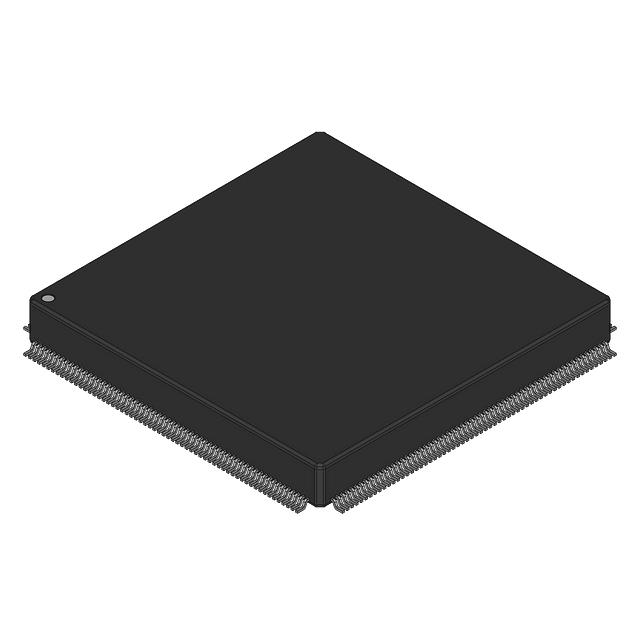
Virtex® Field Programmable Gate Array (FPGA) IC 166 81920 10800 240-BFQFP Exposed Pad |
|---|---|
| Quantity | 595 Available (as of June 15, 2026) |

| Product Category | Field Programmable Gate Array (FPGA) |
|---|---|
| Manufacturer | AMD |
| Manufacturing Status | Obsolete |
| Manufacturer Standard Lead Time | Contact Us |
| Datasheet |
Specifications & Environmental
| Device Package | 240-PQFP (32x32) | Grade | Industrial | Operating Temperature | -40°C – 100°C | ||
|---|---|---|---|---|---|---|---|
| Package / Case | 240-BFQFP Exposed Pad | Number of I/O | 166 | Voltage | 2.375 V - 2.625 V | ||
| Mounting Method | Surface Mount | RoHS Compliance | RoHS non-compliant | REACH Compliance | REACH Unaffected | ||
| Moisture Sensitivity Level | 3 (168 Hours) | Number of LABs/CLBs | 2400 | Number of Logic Elements/Cells | 10800 | ||
| Number of Gates | 468252 | ECCN | 3A001A7B | HTS Code | 8542.39.0001 | ||
| Qualification | N/A | Total RAM Bits | 81920 |
Overview of XCV400-4HQ240I – Virtex® Field Programmable Gate Array (FPGA) IC
The XCV400-4HQ240I is an industrial-grade Virtex SRAM-based FPGA offering a high-density programmable logic solution in a 240-BFQFP exposed pad surface-mount package. It combines a flexible logic fabric with on-chip RAM and multi-standard I/O to address embedded system, interface, and prototyping applications.
As part of the Virtex family, series-level capabilities include a 0.22 μm 5-layer-metal process and system-level features such as clock-management resources and multi-standard I/O. The device is optimized for designs that require re-programmability, dense logic, and broad I/O support within an industrial temperature range.
Key Features
- Logic Capacity — 10,800 logic elements (equivalent) and 468,252 gates provide substantial programmable logic for medium-complexity designs.
- Embedded Memory — Total on-chip RAM of 81,920 bits (approximately 0.082 Mbits) supports local buffering, look-up tables, and small data stores.
- I/O Resources — 166 general-purpose I/O pins and multi-standard SelectIO interfaces support a wide range of external device connectivity and high-performance interface standards.
- Clock Management — Series features include four dedicated delay-locked loops (DLLs), four primary low-skew global clock distribution nets, and 24 secondary local clock nets for advanced clock control and distribution.
- Flexible Logic Architecture — Dedicated carry logic, multiplier support, cascade chains, and configurable LUTs enable efficient implementation of arithmetic, wide-input functions, and embedded memories.
- Configuration and Re-programmability — SRAM-based in-system configuration with unlimited re-programmability and multiple programming modes (SelectMAP™, slave serial, master serial, and JTAG) for development and updates.
- Package & Mounting — Surface-mount 240-BFQFP exposed pad package (supplier package: 240-PQFP 32×32) for board-level integration.
- Power & Environment — Voltage supply range from 2.375 V to 2.625 V and rated operating temperature from −40 °C to 100 °C for industrial deployments.
- Process & Test — Implemented in a 0.22 μm, 5-layer-metal CMOS process and 100% factory tested to ensure device consistency.
- Compliance — RoHS compliant.
Typical Applications
- Embedded System Prototyping — Use the device for FPGA-based prototypes and iterative development where re-programmability and dense logic are required.
- High-density Logic Implementations — Implement mid-range logic functions, arithmetic blocks, and control logic using the device’s 10,800 logic elements and dedicated arithmetic resources.
- Interface & Protocol Bridging — Leverage multi-standard SelectIO and 166 I/Os for protocol conversion, board-level bridging, and peripheral interfacing.
- PCI / Compact PCI Systems — Series-level support for 66-MHz PCI and hot-swappable Compact PCI environments make it suitable for legacy PCI-based interfacing (series capability).
- On-board Memory Acceleration — Use embedded RAM and configurable LUT memory for local buffering and small, fast data storage needs.
Unique Advantages
- Substantial Logic Density: 10,800 logic elements enable integration of multiple functions on a single device, reducing external component count.
- Versatile On-chip Memory: Approximately 81,920 bits of embedded RAM and configurable LUT-based memory modes provide flexible storage options for buffers and state machines.
- Robust Clocking Resources: Multiple DLLs and a hierarchical clock distribution network simplify timing architecture for complex designs.
- Flexible Configuration: SRAM-based in-system programming with multiple modes supports development, field updates, and iterative design cycles.
- Industrial Temperature Range: Rated from −40 °C to 100 °C for deployment in temperature-variable industrial environments.
- Board-level Integration: 240-BFQFP exposed pad surface-mount package offers a compact footprint and standard PCB assembly compatibility.
Why Choose XCV400-4HQ240I?
The XCV400-4HQ240I combines a mid-range logic capacity with on-chip RAM, extensive I/O, and series-level clock-management features to deliver a flexible platform for embedded designs, interface bridging, and prototyping work. Its industrial temperature rating and surface-mount exposed pad package make it suitable for production systems that require reliable, re-programmable logic in a compact form factor.
This device is well suited to design teams and procurement groups seeking a proven Virtex-family FPGA solution that balances programmable logic density, configurable memory, and a broad set of system-level capabilities backed by the device family’s documented features and factory testing.
If you need pricing, availability, or a formal quote for XCV400-4HQ240I, request a quote or submit an inquiry and our team will respond with procurement details and lead-time information.


Date Founded: 1969
Headquarters: Santa Clara, California, USA
Employees: 25,000+
Revenue: $22.68 Billion
Certifications and Memberships: ISO9001:2015, RoHS, REACH


