
XCV400-5BG560I
| Part Description |
Virtex® Field Programmable Gate Array (FPGA) IC 404 81920 10800 560-LBGA Exposed Pad, Metal |
|---|---|
| Quantity | 933 Available (as of June 14, 2026) |

| Product Category | Field Programmable Gate Array (FPGA) |
|---|---|
| Manufacturer | AMD |
| Manufacturing Status | Obsolete |
| Manufacturer Standard Lead Time | Contact Us |
| Datasheet |
Specifications & Environmental
| Device Package | 560-MBGA (42.5x42.5) | Grade | Industrial | Operating Temperature | -40°C – 100°C | ||
|---|---|---|---|---|---|---|---|
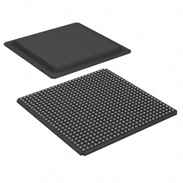
| Package / Case | 560-LBGA Exposed Pad, Metal | Number of I/O | 404 | Voltage | 2.375 V - 2.625 V | ||
| Mounting Method | Surface Mount | RoHS Compliance | RoHS non-compliant | REACH Compliance | REACH Unaffected | ||
| Moisture Sensitivity Level | 3 (168 Hours) | Number of LABs/CLBs | 2400 | Number of Logic Elements/Cells | 10800 | ||
| Number of Gates | 468252 | ECCN | 3A991D | HTS Code | 8542.39.0001 | ||
| Qualification | N/A | Total RAM Bits | 81920 |
Overview of XCV400-5BG560I – Virtex® FPGA, 10,800 logic elements, 560-LBGA
The XCV400-5BG560I is a Virtex® Field Programmable Gate Array (FPGA) offering a balanced combination of logic capacity, on-chip memory, and I/O density for industrial applications. This SRAM-based, in-system configurable device delivers 10,800 logic elements, approximately 81.9 kbits of embedded RAM, and 404 user I/O to support medium-complexity digital designs.
Designed for industrial use, the device operates across a wide temperature range and uses a narrow core supply window, providing predictable integration for systems that require reprogrammability, clock management, and dense I/O in a compact 560-LBGA package.
Key Features
- Core Logic 10,800 logic elements and 468,252 gates provide the programmable fabric for custom digital functions and algorithm implementation.
- Embedded Memory Approximately 81,920 bits of on-chip RAM enable local buffering, lookup tables, and small data stores for timing-critical logic.
- I/O Density 404 user I/O pins support complex interfacing requirements and allow multiple simultaneous external connections from a single device.
- Clock and Timing Built-in clock-management features include multiple delay-locked loops (DLLs) and dedicated global/local clock networks to support advanced clock control and distribution.
- Configurable Architecture SRAM-based, in-system configuration permits unlimited reprogramming and multiple programming modes for iterative development and field updates.
- Performance Architecture and process choices support system-level performance suitable for applications requiring higher clock rates and throughput.
- Package & Power 560-LBGA exposed pad, metal package (supplier package: 560-MBGA, 42.5 × 42.5 mm) in a surface-mount form factor. Core supply voltage specified at 2.375 V to 2.625 V.
- Industrial Reliability Industrial-grade operating temperature range from −40 °C to 100 °C and 100% factory testing support deployment in demanding environments.
- System Support Features such as IEEE 1149.1 boundary-scan, die-temperature sensing, dedicated arithmetic support (carry logic and multipliers), and hierarchical routing enhance system integration and testability.
Typical Applications
- PCI and CompactPCI Systems Supports PCI-compliant interfaces and hot-swappable CompactPCI configurations where reprogrammable logic and dense I/O are required.
- Industrial Control and Automation Industrial-grade temperature range and robust packaging make the device suitable for motor control, machine vision pre-processing, and fieldbus interfacing in factory environments.
- Protocol Bridging and Interface Concentration High I/O count and flexible I/O standards enable protocol conversion, interface aggregation, and custom bus bridging tasks.
- Prototyping and In-System Reconfiguration SRAM-based, unlimited reprogramming modes support iterative development, algorithm updates, and in-field feature upgrades.
Unique Advantages
- Reprogrammable SRAM Architecture: Allows unlimited in-system updates to accelerate development cycles and enable field feature enhancements.
- High I/O Count: 404 user I/O pins reduce external multiplexing and simplify PCB routing for multi-channel designs.
- Compact, Thermally-Considered Package: 560-LBGA exposed-pad metal package provides a compact footprint with thermal conduction suitable for board-level integration.
- Integrated Clock Management: Multiple DLLs and hierarchical clock resources enable fine-grained timing control for high-performance synchronous designs.
- Industrial Temperature Range: Rated from −40 °C to 100 °C to meet the environmental needs of industrial applications.
- Proven System Features: Boundary-scan, die-temperature sensing, dedicated arithmetic support, and factory testing simplify system bring-up and verification.
Why Choose XCV400-5BG560I?
The XCV400-5BG560I positions itself as a versatile, industrial-grade FPGA for designers who need a reliable, reprogrammable platform with substantial logic capacity, significant I/O density, and on-chip memory. Its combination of configurable logic, embedded RAM, clock management, and system-level features supports a wide range of embedded and infrastructure-focused designs.
Ideal for engineering teams implementing medium-complexity digital systems, custom interface logic, or field-updatable functionality, this device offers the predictability of a narrow core voltage range, rugged operating temperatures, and a compact LBGA package for dense board-level designs.
Request a quote or submit your project requirements to receive pricing and availability information for the XCV400-5BG560I.


Date Founded: 1969
Headquarters: Santa Clara, California, USA
Employees: 25,000+
Revenue: $22.68 Billion
Certifications and Memberships: ISO9001:2015, RoHS, REACH


