
XCV400-5FG676C
| Part Description |
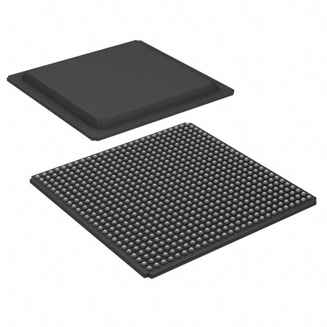
Virtex® Field Programmable Gate Array (FPGA) IC 404 81920 10800 676-BGA |
|---|---|
| Quantity | 173 Available (as of June 10, 2026) |
| Product Category | Field Programmable Gate Array (FPGA) |
|---|---|
| Manufacturer | AMD |
| Manufacturing Status | Obsolete |
| Manufacturer Standard Lead Time | Contact Us |
| Datasheet |
Specifications & Environmental
| Device Package | 676-FBGA (27x27) | Grade | Commercial | Operating Temperature | 0°C – 85°C | ||
|---|---|---|---|---|---|---|---|
| Package / Case | 676-BGA | Number of I/O | 404 | Voltage | 2.375 V - 2.625 V | ||
| Mounting Method | Surface Mount | RoHS Compliance | RoHS non-compliant | REACH Compliance | REACH Unaffected | ||
| Moisture Sensitivity Level | 3 (168 Hours) | Number of LABs/CLBs | 2400 | Number of Logic Elements/Cells | 10800 | ||
| Number of Gates | 468252 | ECCN | 3A991D | HTS Code | 8542.39.0001 | ||
| Qualification | N/A | Total RAM Bits | 81920 |
Overview of XCV400-5FG676C – Virtex® FPGA – 676‑BGA, 10,800 logic elements, 404 I/O
The XCV400-5FG676C is an SRAM-based Virtex® Field Programmable Gate Array (FPGA) offered in a 676-ball BGA package. It delivers a high-density, reprogrammable logic fabric with 10,800 logic elements and 2,400 configurable logic blocks (CLBs) arranged for complex digital designs.
Designed for systems that require abundant I/O, embedded memory, and advanced clock management, this device is suited to applications needing flexible in-system configuration, multi-standard I/O interfaces, and a hierarchical memory architecture.
Key Features
- Core Logic — 10,800 logic elements implemented across a 2,400 CLB array, enabling high-density programmable logic and complex combinational/sequential functions.
- On-chip Memory — Approximately 81,920 bits of embedded RAM plus support for configurable LUT-based RAM and 4k-bit dual-ported RAM blocks for flexible storage and buffering.
- I/O Capacity — 404 available I/O pins to support wide parallel interfaces and multiple external connections.
- Clock Management — Built-in clock-management circuitry including four dedicated delay-locked loops (DLLs) and multiple global/local clock nets for low-skew clock distribution.
- Dedicated Arithmetic Support — Dedicated carry logic and multiplier support to accelerate arithmetic and DSP-like functions.
- Configuration & Re-programmability — SRAM-based in-system configuration with unlimited re-programmability and multiple programming modes.
- Process & Quality — Fabricated on a 0.22 μm, 5-layer-metal CMOS process and 100% factory tested.
- Package & Power — 676‑BGA (27 × 27 mm) package; specified supply voltage range 2.375 V to 2.625 V.
- Operating Range — Commercial grade operation from 0 °C to 85 °C.
- Design Integration — Hierarchical routing and internal 3-state bussing with IEEE 1149.1 boundary-scan logic for board-level testability.
Typical Applications
- PCI and Compact PCI systems — Suitable for designs requiring 66-MHz PCI compliance and hot‑swappable Compact PCI implementations as noted in the device family documentation.
- High-density digital processing — Implements complex logic functions and arithmetic engines using dedicated carry and multiplier resources.
- Memory-intensive interfaces — Ideal for designs that connect to external high-performance RAMs or ZBTRAM devices and that leverage the device’s embedded RAM and configurable LUT memory.
- In-system configurable logic — Reprogrammable FPGA fabrics for prototyping, iterative development, and field updates via multiple configuration modes.
Unique Advantages
- High integration density: 10,800 logic elements provide substantial logic capacity in a single 676‑BGA package, reducing board-level component count.
- Extensive I/O support: 404 I/O pins allow direct interfacing with broad parallel buses and multiple peripheral devices.
- Flexible memory architecture: Approximately 81,920 bits of on-chip RAM plus configurable LUT-based RAM options enable varied storage configurations without adding external memory.
- Robust clock control: Four DLLs and multiple global/local clock nets enable precise timing control for multi-clock-domain designs.
- Re-programmable in-system: SRAM-based configuration supports unlimited re-programmability and multiple programming modes for design iteration and field updates.
- Manufacturing quality: Fabricated in a 0.22 μm, 5-layer-metal process and 100% factory tested for predictable production reliability.
Why Choose XCV400-5FG676C?
The XCV400-5FG676C combines a high-density FPGA fabric with extensive I/O, embedded memory, and advanced clock-management features to address complex digital designs that require in-system flexibility and reliable production testing. Its commercial-grade temperature range and defined supply voltage make it straightforward to integrate into a wide range of system boards.
This device is well suited for engineering teams needing a reprogrammable, high-capacity logic solution with strong support for memory interfaces, deterministic clocking, and a proven manufacturing process. The combination of logic capacity, on-chip memory, and configuration flexibility provides a scalable platform for iterative development and deployment.
Request a quote or submit a product inquiry to receive pricing, availability, and technical support for the XCV400-5FG676C. Our team can provide the information needed to evaluate this FPGA for your next design.


Date Founded: 1969
Headquarters: Santa Clara, California, USA
Employees: 25,000+
Revenue: $22.68 Billion
Certifications and Memberships: ISO9001:2015, RoHS, REACH


