
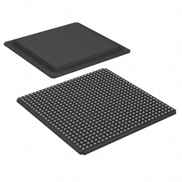
XCV400-6FG676C
| Part Description |
Virtex® Field Programmable Gate Array (FPGA) IC 404 81920 10800 676-BGA |
|---|---|
| Quantity | 419 Available (as of June 10, 2026) |

| Product Category | Field Programmable Gate Array (FPGA) |
|---|---|
| Manufacturer | AMD |
| Manufacturing Status | Obsolete |
| Manufacturer Standard Lead Time | Contact Us |
| Datasheet |
Specifications & Environmental
| Device Package | 676-FBGA (27x27) | Grade | Commercial | Operating Temperature | 0°C – 85°C | ||
|---|---|---|---|---|---|---|---|
| Package / Case | 676-BGA | Number of I/O | 404 | Voltage | 2.375 V - 2.625 V | ||
| Mounting Method | Surface Mount | RoHS Compliance | RoHS non-compliant | REACH Compliance | REACH Unaffected | ||
| Moisture Sensitivity Level | 3 (168 Hours) | Number of LABs/CLBs | 2400 | Number of Logic Elements/Cells | 10800 | ||
| Number of Gates | 468252 | ECCN | 3A991D | HTS Code | 8542.39.0001 | ||
| Qualification | N/A | Total RAM Bits | 81920 |
Overview of XCV400-6FG676C – Virtex® Field Programmable Gate Array (FPGA) IC 404 81920 10800 676-BGA
The XCV400-6FG676C is a Virtex® SRAM-based Field Programmable Gate Array optimized for high-performance, high-capacity programmable logic applications. It features a flexible FPGA architecture with 10,800 logic elements and approximately 81,920 bits of on-chip RAM, making it suitable for complex logic, interface bridging, and system prototyping in commercial electronic designs.
Designed for integration into systems requiring dense logic, multiple I/O standards and advanced clock management, this device provides a balance of performance, capacity and configuration flexibility while operating from a 2.375 V to 2.625 V supply and a commercial temperature range of 0 °C to 85 °C.
Key Features
- Core Density and Logic — 10,800 logic elements and 468,252 system gates provide substantial programmable logic capacity for medium- to high-complexity designs.
- On‑Chip Memory — Approximately 81,920 bits of embedded block RAM plus LUTs that can be configured as various small RAM or shift-register structures for flexible local storage and buffering.
- I/O and Package — 404 user I/Os in a 676-BGA package; supplier device package listed as 676-FBGA (27×27). Surface-mount mounting type for PCB integration.
- Clock and Timing — Built-in clock-management circuitry with four dedicated delay-locked loops (DLLs), four primary low-skew global clock nets and 24 secondary local clock nets to support complex timing domains; documented system performance up to 200 MHz.
- High‑Speed Interfaces — Multi-standard SelectIO™ interfaces supporting a range of interface standards and direct connectivity options for external memory devices; includes 66-MHz PCI compliance and hot‑swappable Compact PCI support noted in the specification.
- Arithmetic and Logic Support — Dedicated carry logic and multiplier support plus cascade chains and abundant registers for high-speed arithmetic and wide-function implementations.
- Configuration and Reliability — SRAM-based in-system configuration with multiple programming modes (SelectMAP™, slave serial, master serial, JTAG); includes IEEE 1149.1 boundary-scan and a die-temperature sensor diode. 0.22 μm 5-layer-metal process and 100% factory tested.
- Power and Operating Conditions — Voltage supply range 2.375 V to 2.625 V; commercial operating temperature range 0 °C to 85 °C; grade: Commercial.
Typical Applications
- PCI/CompactPCI Systems — Implements custom bus interfaces and bridging logic with documented 66‑MHz PCI compliance and hot‑swappable Compact PCI capability.
- High‑Speed Interface Bridging — Multi-standard SelectIO™ and dedicated I/O resources enable protocol translation and interface aggregation for telecom and networking peripherals.
- Embedded Processing and Prototyping — Large logic capacity and configurable on-chip RAM make the device suitable for embedded logic prototyping, hardware acceleration and custom IP development.
- Memory Controller and Buffering — Configurable LUT RAMs and 4k-bit dual-ported RAM blocks support local buffering and fast interfaces to external high-performance RAMs.
Unique Advantages
- Substantial Logic Capacity: 10,800 logic elements and over 468,000 gates provide headroom for complex state machines, datapaths and control logic without immediate need for larger families.
- Flexible Clocking: Four DLLs and multiple global/local clock nets simplify multi‑domain timing and low‑skew distribution for performance-sensitive designs.
- Versatile Memory Topology: LUTs configurable as RAM plus dedicated block RAM options allow designers to tailor on‑chip storage to application needs.
- Multiple Configuration Modes: SRAM-based in-system programmability with several configuration modes enables rapid development iterations and field re-programmability.
- Industry-Scale Process and Test: Fabricated on a 0.22 μm 5-layer-metal process and 100% factory tested to support predictable integration into commercial products.
Why Choose XCV400-6FG676C?
The XCV400-6FG676C delivers a well-balanced combination of logic density, configurable memory and robust clocking resources for commercial embedded and interface-centric designs. Its SRAM-based architecture and multiple configuration modes support iterative development and in-system updates, while the documented I/O count and package make it straightforward to integrate on modern PCBs.
This device is suited to teams needing a commercially graded FPGA with medium‑to‑high logic capacity and flexible I/O for prototyping, interface bridging, and system integration where documented electrical and timing features align with project requirements.
Request a quote or submit your RFQ to receive pricing, availability and additional procurement information for the XCV400-6FG676C.


Date Founded: 1969
Headquarters: Santa Clara, California, USA
Employees: 25,000+
Revenue: $22.68 Billion
Certifications and Memberships: ISO9001:2015, RoHS, REACH


