
XCV400E-6BG560C
| Part Description |
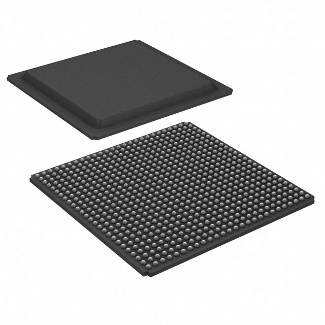
Virtex®-E Field Programmable Gate Array (FPGA) IC 404 163840 10800 560-LBGA Exposed Pad, Metal |
|---|---|
| Quantity | 555 Available (as of June 15, 2026) |

| Product Category | Field Programmable Gate Array (FPGA) |
|---|---|
| Manufacturer | AMD |
| Manufacturing Status | Obsolete |
| Manufacturer Standard Lead Time | Contact Us |
| Datasheet |
Specifications & Environmental
| Device Package | 560-MBGA (42.5x42.5) | Grade | Commercial | Operating Temperature | 0°C – 85°C | ||
|---|---|---|---|---|---|---|---|
| Package / Case | 560-LBGA Exposed Pad, Metal | Number of I/O | 404 | Voltage | 1.71 V - 1.89 V | ||
| Mounting Method | Surface Mount | RoHS Compliance | RoHS non-compliant | REACH Compliance | REACH Unaffected | ||
| Moisture Sensitivity Level | 3 (168 Hours) | Number of LABs/CLBs | 2400 | Number of Logic Elements/Cells | 10800 | ||
| Number of Gates | 569952 | ECCN | 3A991D | HTS Code | 8542.39.0001 | ||
| Qualification | N/A | Total RAM Bits | 163840 |
Overview of XCV400E-6BG560C – Virtex®-E Field Programmable Gate Array (FPGA) IC 404 163840 10800 560-LBGA Exposed Pad, Metal
The XCV400E-6BG560C is a Virtex®-E series 1.8 V FPGA in a 560-LBGA exposed-pad package, designed for commercial-grade embedded and interface applications. It combines reprogrammable SRAM-based logic with a high pin-count I/O array to support complex glue-logic, protocol bridging, and high-density digital processing.
This device offers a balance of logic capacity, on-chip memory and I/O resources—making it suitable for designs that require flexible, field-upgradeable logic at a commercial temperature range.
Key Features
- Core Architecture Virtex‑E family FPGA architecture with SRAM-based in-system configuration and unlimited re-programmability.
- Logic Capacity Approximately 10,800 logic elements (listed as 10800 logic element cells) and 569,952 gates to implement medium-density logic functions.
- On-Chip Memory Approximately 163,840 bits of embedded RAM (~160 Kbits) for distributed and block memory needs within the FPGA fabric.
- I/O and Signaling 404 user I/O pins in this package; the Virtex‑E family supports high-performance SelectI/O+ standards and differential signaling (LVDS, BLVDS, LVPECL) where applicable.
- Clock Management Series-level clock management includes multiple digital DLLs for clock multiply/divide and duty-cycle control to support synchronous interfaces.
- Power and Supply Internal supply (VCCINT) specified at 1.71 V to 1.89 V for the FPGA core.
- Package and Mounting 560‑LBGA exposed pad, metal package (supplier device package: 560‑MBGA, 42.5 × 42.5 mm) designed for surface-mount assembly.
- Environmental and Grade Commercial grade device with an operating temperature range of 0 °C to 85 °C and RoHS compliance.
Typical Applications
- High‑speed interface bridging Implement protocol translation and bus bridging where a large number of I/Os and flexible signaling standards are required.
- Embedded processing logic Offload custom control and data-path functions using the device’s logic elements and on-chip RAM for buffering and temporary storage.
- Memory interface control Act as an interface controller for external memory systems leveraging the family’s support for high-performance memory interfaces.
- In‑system reconfigurable solutions Deploy field-upgradable logic for iterative product development, firmware updates, or feature extensions without hardware changes.
Unique Advantages
- Balanced logic and memory resources: The combination of ~10,800 logic elements and ~163,840 bits of embedded RAM lets you map moderate-complexity designs without external glue logic.
- High I/O density: 404 I/O pins in a compact 560‑LBGA package support complex multi-channel interfaces and routing flexibility.
- Reprogrammability and development agility: SRAM-based in-system configuration enables unlimited re-programmability for firmware updates and design iteration.
- Commercial-temperature operation: Specified for 0 °C to 85 °C to match a wide range of commercial embedded applications.
- Industry-standard packaging: Surface-mount 560-MBGA (42.5 × 42.5 mm) package provides a robust platform for automated assembly and thermal management via the exposed pad.
- Regulatory readiness: RoHS compliant for global commercial product manufacturing.
Why Choose XCV400E-6BG560C?
The XCV400E-6BG560C packages Virtex‑E family capabilities into a compact, surface-mount 560‑LBGA form factor that suits commercial embedded designs requiring reprogrammable logic, significant I/O, and on-chip RAM. Its combination of approximately 10,800 logic elements, 404 I/Os, and reprogrammable SRAM fabric supports applications ranging from interface controllers to custom data processing blocks.
Choose this device when you need a commercially graded FPGA that provides field-upgradeability, a high I/O count, and documented supply and temperature limits for reliable integration into production systems.
Request a quote or submit a pricing inquiry for XCV400E-6BG560C to receive availability and ordering information.


Date Founded: 1969
Headquarters: Santa Clara, California, USA
Employees: 25,000+
Revenue: $22.68 Billion
Certifications and Memberships: ISO9001:2015, RoHS, REACH


