
XCV400E-6BG560I
| Part Description |
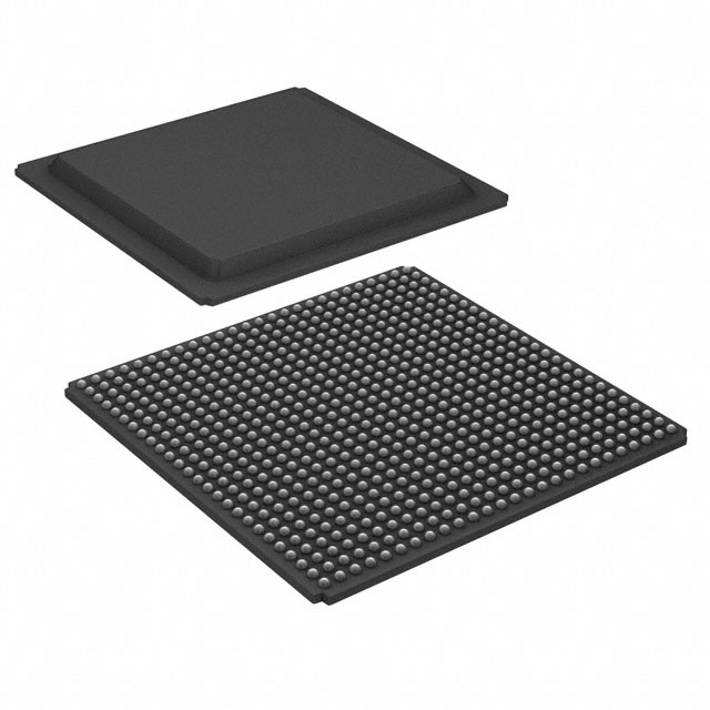
Virtex®-E Field Programmable Gate Array (FPGA) IC 404 163840 10800 560-LBGA Exposed Pad, Metal |
|---|---|
| Quantity | 296 Available (as of October 8, 2026) |

| Product Category | Field Programmable Gate Array (FPGA) |
|---|---|
| Manufacturer | AMD |
| Manufacturing Status | Obsolete |
| Manufacturer Standard Lead Time | Contact Us |
| Datasheet |
Specifications & Environmental
| Device Package | 560-MBGA (42.5x42.5) | Grade | Industrial | Operating Temperature | -40°C – 100°C | ||
|---|---|---|---|---|---|---|---|
| Package / Case | 560-LBGA Exposed Pad, Metal | Number of I/O | 404 | Voltage | 1.71 V - 1.89 V | ||
| Mounting Method | Surface Mount | RoHS Compliance | RoHS non-compliant | REACH Compliance | REACH Unaffected | ||
| Moisture Sensitivity Level | 3 (168 Hours) | Number of LABs/CLBs | 2400 | Number of Logic Elements/Cells | 10800 | ||
| Number of Gates | 569952 | ECCN | 3A991D | HTS Code | 8542.39.0001 | ||
| Qualification | N/A | Total RAM Bits | 163840 |
Overview of XCV400E-6BG560I – Virtex®-E FPGA, 560-LBGA, Industrial Grade
The XCV400E-6BG560I is a Virtex®-E field programmable gate array (FPGA) supplied in a 560-LBGA exposed-pad metal package. It combines medium-density programmable logic with a high I/O count and on-chip RAM to support complex digital designs.
Built on the Virtex-E architecture, this device is aimed at applications requiring reprogrammable logic, substantial I/O bandwidth, and operation across an industrial temperature range. Key on-device resources include approximately 10,800 logic elements, roughly 163,840 bits of embedded memory, and 404 user I/O pins.
Key Features
- Logic Capacity Approximately 10,800 logic elements (about 569,952 system gates) for implementing custom digital logic and control functions.
- On-chip Memory Approximately 163,840 bits of embedded RAM for local buffering, state storage, and small data structures.
- I/O and Interface Capability 404 user I/O pins provided in the package; Virtex‑E family features include support for a variety of high-performance differential signalling standards (family-level capability).
- Core Supply Voltage Internal core supply specified at 1.71 V to 1.89 V, matching the Virtex‑E 1.8 V design point.
- Package and Mounting 560-LBGA exposed pad, metal package (supplier device package: 560-MBGA, 42.5 × 42.5 mm) for high I/O density; surface-mount mounting type.
- Operating Range Industrial-grade operation with an ambient temperature range of −40 °C to 100 °C.
- SRAM-Based, In-System Reprogrammability Supports SRAM-based in-system configuration for unlimited reprogramming (family feature described in product documentation).
- Clock and Timing Features (Family-level) Virtex‑E family documentation describes advanced clock management including multiple DLLs and support for high-speed clock inputs (refer to family datasheet for details).
- RoHS Compliance Device is RoHS compliant.
Typical Applications
- PCI and Bus Interface Controllers Implement PCI-compliant bus interfaces and bridging logic leveraging the device’s I/O capacity and Virtex‑E family support for 3.3 V PCI signaling.
- High-Speed Memory Controllers Ideal for custom memory interface logic and controllers that require on-chip RAM and support for external memory protocols referenced in the family documentation.
- Protocol Conversion and Data Aggregation Use the device’s abundant I/O and programmable logic to consolidate, translate, or route high-bandwidth digital signals between subsystems.
- Embedded System Prototyping Reprogrammability and moderate logic density make this FPGA suitable for iterative development and functional prototyping of embedded digital subsystems.
Unique Advantages
- Balanced Logic Density and I/O: Around 10,800 logic elements combined with 404 I/O pins gives a practical balance for mid-range designs that need significant external connectivity without very large die sizes.
- Industrial Temperature Range: Rated for −40 °C to 100 °C operation, supporting deployment in a broad set of industrial environments.
- High-Density BGA Packaging: The 560-LBGA exposed-pad metal package enables high pin count and thermal dissipation in a compact surface-mount footprint.
- Reprogrammable SRAM Architecture: SRAM-based in-system configuration enables iterative development and field updates without hardware changes.
- Directly Verifiable Power Requirements: Core supply range of 1.71 V to 1.89 V allows straightforward power budgeting and integration into existing 1.8 V subsystem rails.
- Toolchain and Family Support (Documentation): The Virtex‑E family is documented with development-system support and reference design resources described in the product literature.
Why Choose XCV400E-6BG560I?
The XCV400E-6BG560I delivers a practical combination of programmable logic, embedded RAM, and high I/O count in a robust industrial-grade BGA package. Its 1.8 V core architecture and SRAM-based reprogrammability make it suitable for mid-density FPGA tasks where design iteration and field updates matter.
This device is well suited to engineers building PCI interfaces, memory controllers, protocol bridges, or embedded prototypes that require deterministic operating temperatures, a defined power envelope, and a compact high-pin-count package. Documentation for the Virtex‑E family provides additional architectural and development-system details to support integration and deployment.
Request a quote or submit a product inquiry to obtain pricing, lead times, and availability for the XCV400E-6BG560I.






















Date Founded: 1969
Headquarters: Santa Clara, California, USA
Employees: 25,000+
Revenue: $22.68 Billion
Certifications and Memberships: ISO9001:2015, RoHS, REACH











