
XCV400E-6FG676C
| Part Description |
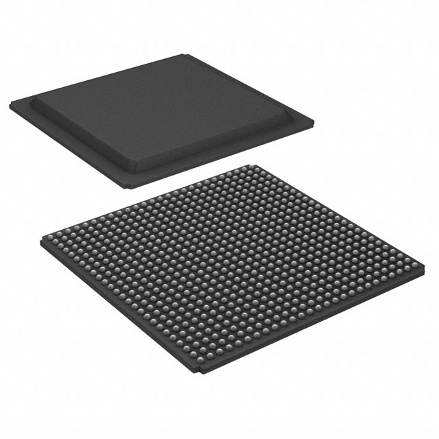
Virtex®-E Field Programmable Gate Array (FPGA) IC 404 163840 10800 676-BGA |
|---|---|
| Quantity | 525 Available (as of October 8, 2026) |
| Product Category | Field Programmable Gate Array (FPGA) |
|---|---|
| Manufacturer | AMD |
| Manufacturing Status | Obsolete |
| Manufacturer Standard Lead Time | Contact Us |
| Datasheet |
Specifications & Environmental
| Device Package | 676-FBGA (27x27) | Grade | Commercial | Operating Temperature | 0°C – 85°C | ||
|---|---|---|---|---|---|---|---|
| Package / Case | 676-BGA | Number of I/O | 404 | Voltage | 1.71 V - 1.89 V | ||
| Mounting Method | Surface Mount | RoHS Compliance | RoHS non-compliant | REACH Compliance | REACH Unaffected | ||
| Moisture Sensitivity Level | 3 (168 Hours) | Number of LABs/CLBs | 2400 | Number of Logic Elements/Cells | 10800 | ||
| Number of Gates | 569952 | ECCN | 3A991D | HTS Code | 8542.39.0001 | ||
| Qualification | N/A | Total RAM Bits | 163840 |
Overview of XCV400E-6FG676C – Virtex®-E Field Programmable Gate Array (FPGA) IC 404 163840 10800 676-BGA
The XCV400E-6FG676C is a Virtex®-E series FPGA provided by AMD in a 676-ball FBGA package. It combines programmable logic, a significant I/O count and on-chip memory for mid-density, reconfigurable designs.
Designed for commercial applications, this device operates from a 1.71 V to 1.89 V core supply, supports up to 404 I/Os, and includes 10,800 logic elements with approximately 0.16 Mbits of embedded memory, offering a balance of logic capacity, I/O bandwidth and on-chip storage for system integration.
Key Features
- Core & logic 10,800 logic elements and approximately 569,952 equivalent gates provide the programmable fabric for implementing custom logic and control functions.
- Embedded memory Approximately 0.16 Mbits of on-chip RAM (163,840 bits) for distributed or block memory needs within the design.
- I/O capacity & signaling (family-level) 404 user I/Os enable high pin-count interfaces; the Virtex‑E family supports a range of high-performance differential and single-ended signaling standards for flexible system interfacing.
- Performance & clocking (family-level) Built on the Virtex‑E architecture which includes advanced clock-management features and internal performance characteristics suitable for multi-clock designs.
- Package & mounting 676-FBGA (27×27) package case; surface-mount mounting type for standard PCB assembly processes.
- Power & thermal Core supply range 1.71 V to 1.89 V; commercial operating temperature 0 °C to 85 °C.
- Compliance RoHS compliant for regulatory and environmental considerations.
Typical Applications
- PCI and bus bridging Integration into PCI-compliant subsystems and other bus-interface logic where reconfigurable glue logic and protocol adaptation are required.
- Memory interface controllers Implement controllers and interface logic for external memories and high-speed SRAM/DRAM connections using the device's logic and I/O resources.
- Embedded system glue logic Consolidate multiple discrete components into programmable logic for control, timing, and interface adaptation in embedded applications.
- Prototyping and in-system reconfiguration Use the FPGA's reprogrammable fabric to prototype designs and iterate system-level functions without respinning hardware.
Unique Advantages
- High I/O count: 404 I/Os enable dense external connections and support for multiple parallel interfaces.
- Balanced logic and memory: 10,800 logic elements combined with approximately 0.16 Mbits of embedded RAM let designers implement medium-complexity functions with on-chip storage.
- Low-voltage core operation: Narrow core supply range (1.71 V–1.89 V) aligns with low-voltage system architectures.
- Commercial temperature grade: Rated for 0 °C to 85 °C operation to match a wide range of standard commercial products.
- Industry-standard packaging: 676-FBGA (27×27) surface-mount package simplifies integration into modern PCB designs.
- RoHS compliant: Meets RoHS requirements for environmentally conscious product designs.
Why Choose XCV400E-6FG676C?
This FPGA offers a practical balance of logic capacity, embedded memory and high I/O density in a compact 676-FBGA package, making it suitable for designers who need reconfigurable logic and flexible interfacing in commercial applications. Built on the Virtex‑E family architecture, the device leverages proven FPGA capabilities while operating at a low core voltage and within standard commercial temperature ranges.
The XCV400E-6FG676C is a fit for system designers looking to consolidate discrete logic, implement custom interfaces, or prototype complex digital functions with the option of in-system reprogrammability and RoHS-compliant hardware.
Request a quote or submit an inquiry for pricing, availability and lead-time information for the XCV400E-6FG676C.






















Date Founded: 1969
Headquarters: Santa Clara, California, USA
Employees: 25,000+
Revenue: $22.68 Billion
Certifications and Memberships: ISO9001:2015, RoHS, REACH











