
XCV400E-7BG432C
| Part Description |
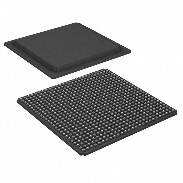
Virtex®-E Field Programmable Gate Array (FPGA) IC 316 163840 10800 432-LBGA Exposed Pad, Metal |
|---|---|
| Quantity | 1,622 Available (as of October 8, 2026) |

| Product Category | Field Programmable Gate Array (FPGA) |
|---|---|
| Manufacturer | AMD |
| Manufacturing Status | Obsolete |
| Manufacturer Standard Lead Time | Contact Us |
| Datasheet |
Specifications & Environmental
| Device Package | 432-MBGA (40x40) | Grade | Commercial | Operating Temperature | 0°C – 85°C | ||
|---|---|---|---|---|---|---|---|
| Package / Case | 432-LBGA Exposed Pad, Metal | Number of I/O | 316 | Voltage | 1.71 V - 1.89 V | ||
| Mounting Method | Surface Mount | RoHS Compliance | RoHS non-compliant | REACH Compliance | REACH Unaffected | ||
| Moisture Sensitivity Level | 3 (168 Hours) | Number of LABs/CLBs | 2400 | Number of Logic Elements/Cells | 10800 | ||
| Number of Gates | 569952 | ECCN | 3A991D | HTS Code | 8542.39.0001 | ||
| Qualification | N/A | Total RAM Bits | 163840 |
Overview of XCV400E-7BG432C – Virtex®-E Field Programmable Gate Array (FPGA), 432-LBGA
The XCV400E-7BG432C is a Virtex®-E family FPGA packaged in a 432-LBGA exposed-pad metal package. It is an SRAM-based, reprogrammable logic device designed for systems requiring high I/O density, flexible interface support and on-chip embedded memory.
Engineered for commercial-grade environments, this device targets high-performance interface designs, memory-interfacing applications and general-purpose reconfigurable logic where a 1.8 V core and extensive I/O are required.
Key Features
- Core Density — 10,800 logic elements (approximate device logic resource) and 569,952 system gates, providing substantial programmable logic for mid-range FPGA designs.
- Embedded Memory — 163,840 bits of on-chip RAM (approximately 0.16 Mbits) for distributed and block memory usage in logic designs.
- I/O Capacity — 316 user I/O pins supporting a broad range of system interfaces and high aggregate bandwidth.
- High-Speed Interfaces — Series-level SelectI/O+™ and differential signalling support including LVDS, BLVDS and LVPECL for high-performance link and clock inputs (from datasheet series information).
- Clock Management — Digital clock management with multiple DLLs for flexible clock multiplication, division and duty-cycle control (series feature).
- PCI Compatibility — Series-level support for PCI-compliant 3.3 V, 32/64-bit 33/66-MHz interfaces (as documented for the Virtex®-E family).
- Supply and Packaging — Internal supply VCCINT: 1.71 V to 1.89 V; 432-LBGA exposed pad metal package (supplier package: 432-MBGA, 40×40); surface-mount mounting type.
- Operating Range and Compliance — Commercial operating temperature 0 °C to 85 °C and RoHS compliant.
Typical Applications
- High-Speed I/O Systems — Use the device's extensive I/O and differential signalling support for high-bandwidth interface implementations and protocol bridging.
- Memory Interface and Controllers — Implement external memory interfaces (DDR SDRAM, ZBT SRAM referenced at the series level) and custom memory controllers using the on-chip RAM and SelectRAM+ architecture.
- PCI-Based Systems — Integrate into PCI-compliant 3.3 V, 32/64-bit 33/66-MHz designs where programmable logic is required.
- Reconfigurable System Prototyping — Leverage SRAM-based in-system reprogramming for iterative development and field updates.
Unique Advantages
- Substantial Logic Resources: 10,800 logic elements and 569,952 gates provide a strong balance of capacity for mid-range FPGA designs.
- Flexible I/O and Signalling: 316 I/Os plus series-level SelectI/O+ and differential signalling support enable a wide range of interface standards and high-speed links.
- Integrated Memory: 163,840 bits of embedded RAM offers local storage for FIFOs, buffers and small lookup tables without external memory.
- Programmable Clocking: Built-in digital clock management (series DLL features) simplifies timing architectures for multi-clock designs.
- Commercial-Grade Robustness: Rated for 0 °C to 85 °C operation and supplied in a 432-LBGA package with exposed pad for reliable surface-mount assembly.
- RoHS Compliant: Meets current RoHS environmental requirements for lead-free assembly processes.
Why Choose XCV400E-7BG432C?
The XCV400E-7BG432C delivers a practical combination of programmable logic capacity, embedded memory and high I/O count in a 432-LBGA package suitable for commercial electronic systems. Its 1.8 V core supply, series-level high-speed interface support and reprogrammable SRAM architecture make it appropriate for designs that require flexible, field-updatable logic and robust clocking options.
This device is well suited to engineers building mid-range FPGA solutions that require predictable commercial-temperature operation, extensive I/O and on-chip memory—offering design scalability within the Virtex®-E family and leveraging the documented series features for interface and clock management.
Request a quote or submit a quote for the XCV400E-7BG432C to check availability and pricing for your next design.






















Date Founded: 1969
Headquarters: Santa Clara, California, USA
Employees: 25,000+
Revenue: $22.68 Billion
Certifications and Memberships: ISO9001:2015, RoHS, REACH











