
XCV400-5HQ240I
| Part Description |
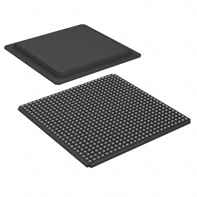
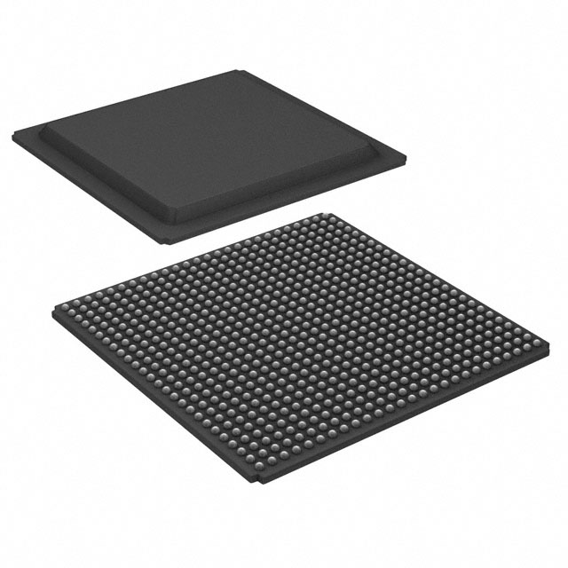
Virtex® Field Programmable Gate Array (FPGA) IC 166 81920 10800 240-BFQFP Exposed Pad |
|---|---|
| Quantity | 990 Available (as of October 8, 2026) |

| Product Category | Field Programmable Gate Array (FPGA) |
|---|---|
| Manufacturer | AMD |
| Manufacturing Status | Obsolete |
| Manufacturer Standard Lead Time | Contact Us |
| Datasheet |
Specifications & Environmental
| Device Package | 240-PQFP (32x32) | Grade | Industrial | Operating Temperature | -40°C – 100°C | ||
|---|---|---|---|---|---|---|---|
| Package / Case | 240-BFQFP Exposed Pad | Number of I/O | 166 | Voltage | 2.375 V - 2.625 V | ||
| Mounting Method | Surface Mount | RoHS Compliance | RoHS non-compliant | REACH Compliance | REACH Unaffected | ||
| Moisture Sensitivity Level | 3 (168 Hours) | Number of LABs/CLBs | 2400 | Number of Logic Elements/Cells | 10800 | ||
| Number of Gates | 468252 | ECCN | 3A001A7B | HTS Code | 8542.39.0001 | ||
| Qualification | N/A | Total RAM Bits | 81920 |
Overview of XCV400-5HQ240I – Virtex Field Programmable Gate Array (FPGA) IC
The XCV400-5HQ240I is a Virtex FPGA manufactured by AMD, delivering high-density, reprogrammable logic for systems requiring flexible hardware implementation. The device integrates approximately 468,252 system gates with 10,800 logic cells and 2,400 configurable logic blocks, making it suitable for complex, high-capacity digital designs.
Designed for applications such as PCI-compliant systems and hot‑swappable Compact PCI modules, the XCV400-5HQ240I combines on-chip memory, multi-standard I/O options, and advanced clock management to enable in-system reconfiguration and rapid design iteration.
Key Features
- Core Logic and Density — Approximately 468,252 system gates, 10,800 logic cells and 2,400 CLBs provide high-capacity programmable logic for complex designs.
- Embedded Memory — 81,920 bits of on-chip RAM for lookup tables and dual-ported RAM configurations; supports hierarchical memory usage for control and data buffering.
- I/O and Interface Flexibility — 166 user I/O pins and Multi‑standard SelectIO support covering 16 high-performance interface standards for broad system connectivity.
- Clock Management — Four dedicated delay-locked loops (DLLs), four primary low‑skew global clock distribution nets and 24 secondary local clock nets for advanced clock control and low-skew distribution.
- Arithmetic and DSP Support — Dedicated carry logic, multiplier support and cascade chains for high-speed arithmetic and wide-function implementations.
- Configuration and Test — SRAM-based in-system configuration with unlimited reprogrammability and four programming modes; includes IEEE 1149.1 boundary-scan logic and a die-temperature sensor diode for diagnostics.
- Process and Quality — Built on a 0.22 μm, 5-layer-metal CMOS process and 100% factory tested for production reliability.
- Package and Environmental — 240-BFQFP exposed pad package (240-PQFP, 32×32), surface-mount mounting; industrial-grade operating range from −40°C to 100°C and supply voltage 2.375 V to 2.625 V. RoHS compliant.
Typical Applications
- PCI systems — Implementation of 66‑MHz PCI‑compliant controllers and interface logic using the device’s high-density logic and multi-standard I/O.
- Compact PCI modules — Hot‑swappable Compact PCI card designs that require reconfigurable logic and robust clocking options.
- In-system reconfigurable designs — Prototyping and production systems that benefit from SRAM-based unlimited reprogramming and multiple configuration modes.
- Mask-programmed replacement — High-capacity programmable alternative to mask-programmed gate arrays where post-production flexibility is required.
Unique Advantages
- High logic capacity: 10,800 logic cells and ~468k system gates enable dense implementations without external ASICs.
- Integrated memory resources: 81,920 bits of embedded RAM reduce external memory requirements for control and buffering tasks.
- Advanced clocking: Multiple DLLs and extensive clock nets simplify timing distribution for synchronous systems.
- Flexible I/O standards: 166 I/Os with SelectIO support across 16 interface standards improve system interoperability.
- Production-ready process: 0.22 μm, 5‑layer metal manufacturing and 100% factory testing support reliable deployment in industrial environments.
- In-system reprogrammability: SRAM-based configuration with four programming modes enables field updates and iterative development.
Why Choose XCV400-5HQ240I?
The XCV400-5HQ240I positions itself as a high-capacity, reprogrammable FPGA suited for applications that demand dense logic, flexible I/O, and robust clock management. Its combination of substantial on-chip memory, dedicated arithmetic resources, and comprehensive configuration options supports both development and production use cases where adaptability and integration matter.
This device is appropriate for engineering teams and system designers building PCI/Compact PCI subsystems, reconfigurable prototypes, or high-density logic replacements for mask-programmed solutions. The industrial temperature rating, exposed-pad PQFP package, and RoHS compliance contribute to long-term deployment reliability across varied environments.
Request a quote or submit an RFQ to obtain pricing, availability, and lead‑time information for the XCV400-5HQ240I.




















Date Founded: 1969
Headquarters: Santa Clara, California, USA
Employees: 25,000+
Revenue: $22.68 Billion
Certifications and Memberships: ISO9001:2015, RoHS, REACH











