IS42S16160B-6BLI
| Part Description |
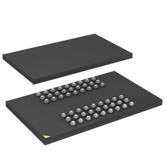
IC DRAM 256MBIT PAR 54LFBGA |
|---|---|
| Quantity | 630 Available (as of June 15, 2026) |

| Product Category | Memory |
|---|---|
| Manufacturer | Integrated Silicon Solution Inc |
| Manufacturing Status | Obsolete |
| Manufacturer Standard Lead Time | Contact Us |
| Datasheet |
Specifications & Environmental
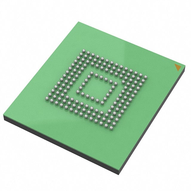
| Device Package | 54-LFBGA (8x13) | Memory Format | DRAM | Technology | SDRAM | ||
|---|---|---|---|---|---|---|---|
| Memory Size | 256 Mbit | Access Time | 5.4 ns | Grade | Industrial | ||
| Clock Frequency | 166 MHz | Voltage | 3V ~ 3.6V | Memory Type | Volatile | ||
| Operating Temperature | -40°C ~ 85°C (TA) | Write Cycle Time Word Page | N/A | Packaging | 54-LFBGA | ||
| Mounting Method | Volatile | Memory Interface | Parallel | Memory Organization | 16M x 16 | ||
| Moisture Sensitivity Level | 3 (168 Hours) | RoHS Compliance | ROHS Compliant | REACH Compliance | REACH Unaffected | ||
| Qualification | N/A | ECCN | EAR99 | HTS Code | 8542.32.0024 |
Overview of IS42S16160B-6BLI – 256 Mbit SDRAM (16M × 16), 54‑LFBGA
The IS42S16160B-6BLI is a 256 Mbit synchronous DRAM organized as 16M × 16 with a parallel memory interface and LVTTL signaling. It uses a pipelined, quad-bank SDRAM architecture to deliver synchronous, burst-oriented memory access for high-speed systems.
Targeted for designs requiring a 3.3V memory solution, this device provides programmable burst operation, internal bank interleaving to hide precharge time, and onboard refresh/self-refresh functions for system reliability across a wide temperature range.
Key Features
- Memory Capacity & Organization — 256 Mbit total capacity organized as 16M × 16 with four internal banks to support interleaved access and efficient burst transfers.
- Performance — Clock frequency up to 166 MHz (‑6 speed grade) with programmable CAS latency (2 or 3 clocks); access time from clock for CL=3 is 5.4 ns.
- Burst & Access Modes — Programmable burst lengths (1, 2, 4, 8, full page) and selectable burst sequence (sequential/interleave); supports burst read/write and burst read/single write operations with burst termination options.
- Interface & Timing — Fully synchronous operation with all signals referenced to the rising clock edge; LVTTL-compatible I/O and random column address every clock cycle during burst access.
- Refresh & Low-Power Modes — Auto Refresh (CBR), Self Refresh, and a power‑down mode; supports 8K refresh cycles every 64 ms for data retention.
- Power — Designed for 3.3V systems (VDD/VDDQ = 3.3V); specified operating supply range 3.0 V to 3.6 V.
- Package & Temperature — 54-ball LFBGA package (8 × 13); industrial operating temperature available with specified range −40 °C to 85 °C (TA).
- Manufacturing Options — Available in lead-free packaging per datasheet options.
Unique Advantages
- Quad‑bank architecture for higher throughput: Four internal banks enable bank interleaving to hide precharge time and maintain continuous data flow during burst transfers.
- Flexible burst control: Programmable burst lengths and sequencing support a range of access patterns for system-level optimization.
- Synchronous, clocked timing: All inputs and outputs are referenced to the rising clock edge for deterministic timing and straightforward system integration.
- Built‑in refresh and low‑power modes: Auto Refresh, Self Refresh and power‑down modes reduce host overhead for memory maintenance and lower standby power.
- Industrial temperature support: Rated for −40 °C to 85 °C, enabling use in systems that require extended temperature operation.
- Compact BGA footprint: 54‑ball LFBGA (8×13) package provides a small form factor for space-constrained board designs.
Why Choose IS42S16160B-6BLI?
The IS42S16160B-6BLI offers a balanced combination of synchronous SDRAM performance and system-oriented features—quad-bank pipelined architecture, programmable burst operation, and built-in refresh/self-refresh—making it suitable for designs that need predictable, high-speed parallel memory. Its 3.3V design, LVTTL interface and industrial temperature range support deployment in a variety of embedded systems that require durable, synchronous DRAM.
Issued by Integrated Silicon Solution, Inc., this 256 Mbit SDRAM provides a verified datasheet, multiple timing options (including a 166 MHz, CL=3 speed grade with 5.4 ns access from clock), and packaging choices to match board-level constraints—helping engineers scale performance while managing board area and thermal considerations.
If you need pricing, lead-time or availability details, request a quote or submit an RFQ to discuss your requirements and obtain a formal quote.