IS42S16800E-7TL-TR
| Part Description |
IC DRAM 128MBIT PAR 54TSOP II |
|---|---|
| Quantity | 907 Available (as of June 15, 2026) |

| Product Category | DRAM Memory |
|---|---|
| Manufacturer | Integrated Silicon Solution Inc |
| Manufacturing Status | Obsolete |
| Manufacturer Standard Lead Time | Contact Us |
| Datasheet |
Specifications & Environmental
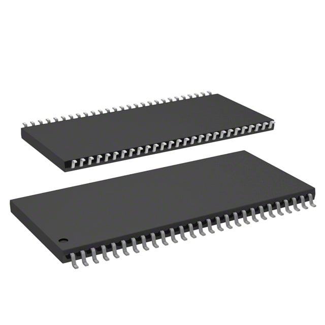
| Device Package | 54-TSOP II | Memory Format | DRAM | Technology | SDRAM | ||
|---|---|---|---|---|---|---|---|
| Memory Size | 128 Mbit | Access Time | 5.4 ns | Grade | Commercial | ||
| Clock Frequency | 143 MHz | Voltage | 3V ~ 3.6V | Memory Type | Volatile | ||
| Operating Temperature | 0°C ~ 70°C (TA) | Write Cycle Time Word Page | N/A | Packaging | 54-TSOP (0.400", 10.16mm Width) | ||
| Mounting Method | Volatile | Memory Interface | Parallel | Memory Organization | 8M x 16 | ||
| Moisture Sensitivity Level | 3 (168 Hours) | RoHS Compliance | ROHS Compliant | REACH Compliance | REACH Unaffected | ||
| Qualification | N/A | ECCN | EAR99 | HTS Code | 8542.32.0002 |
Overview of IS42S16800E-7TL-TR – IC DRAM 128MBIT PAR 54TSOP II
The IS42S16800E-7TL-TR is a 128 Mbit synchronous DRAM (SDRAM) device organized as 8M × 16 with a parallel LVTTL interface. It implements a quad-bank, fully synchronous pipeline architecture to deliver predictable, clock-referenced memory access for board-level systems requiring 128 Mbit DRAM in a compact 54-pin TSOP II package.
Designed for 3.0–3.6 V systems (3.3 V VDD specified in the device datasheet) and a specified operating ambient range of 0°C to 70°C, this SDRAM supports high-throughput burst operations and programmable timing to match system performance requirements.
Key Features
- Core Memory 128 Mbit SDRAM organized as 8M × 16, implemented as a quad-bank DRAM for concurrent row/column operations.
- Synchronous, Clocked Interface Fully synchronous operation with all signals referenced to the rising edge of CLK; supported clock frequencies include 200, 166, 143 and 133 MHz (–7 speed grade corresponds to 143 MHz in the timing table).
- Low Access Time CAS latency and timing options provide access times down to 5.4 ns (CAS Latency = 3 at the –7 grade), enabling low-latency read operations.
- Programmable Burst and CAS Options Programmable burst lengths (1, 2, 4, 8, full page) and selectable burst sequence (Sequential/Interleave); CAS latency programmable to 2 or 3 clocks.
- Refresh and Power Modes Supports Auto Refresh, Self Refresh and CBR Auto Refresh; device requires 4096 refresh cycles every 64 ms as specified.
- Interface and Signaling LVTTL signaling for inputs/outputs and a parallel memory interface optimized for board-level integration.
- Supply and Package Supply range 3.0–3.6 V with 3.3 V VDD indicated in the datasheet; supplied in a 54-pin TSOP II package (0.400", 10.16 mm width) for compact PCB footprints.
Typical Applications
- Board-level SDRAM expansion Provides 128 Mbit of synchronous DRAM capacity for systems requiring parallel memory in a 54-pin TSOP II footprint.
- High-throughput burst buffering Programmable burst lengths and CAS latency options support burst read/write operations for systems that need efficient block transfers.
- 3.3 V memory subsystems Designed for systems operating within a 3.0–3.6 V supply range with LVTTL interface signaling.
Unique Advantages
- Flexible timing and burst control: Programmable CAS latency (2, 3) and burst length/sequence settings let designers tune latency and throughput to match system timing.
- Deterministic synchronous operation: All signals referenced to the positive clock edge yield predictable timing and simplify timing closure for clocked memory systems.
- Compact TSOP II packaging: The 54-pin TSOP II (10.16 mm width) provides a small board footprint for space-constrained designs.
- Standard 3.3 V supply compatibility: Operates within a 3.0–3.6 V supply window with 3.3 V VDD specified in the datasheet to match common system rails.
- Refresh and power management: Built-in Auto Refresh and Self Refresh modes with specified refresh cycle requirements help maintain data integrity while supporting power-saving modes.
Why Choose IS42S16800E-7TL-TR?
The IS42S16800E-7TL-TR provides a compact, fully synchronous 128 Mbit DRAM solution with programmable timing and burst features suited to systems that require predictable, clock-referenced memory performance. Its 54-pin TSOP II package and 3.0–3.6 V supply compatibility make it straightforward to integrate into board-level memory subsystems where space and standard supply voltages are considerations.
This device is appropriate for designers seeking a straightforward SDRAM component with configurable latency and burst behavior, enabling alignment with specific data-transfer and timing requirements while adhering to documented timing parameters and refresh specifications.
Request a quote or submit a pricing inquiry to receive availability and lead-time information for the IS42S16800E-7TL-TR.