IS42S16800E-7TLI-TR
| Part Description |
IC DRAM 128MBIT PAR 54TSOP II |
|---|---|
| Quantity | 167 Available (as of June 17, 2026) |

| Product Category | DRAM Memory |
|---|---|
| Manufacturer | Integrated Silicon Solution Inc |
| Manufacturing Status | Obsolete |
| Manufacturer Standard Lead Time | Contact Us |
| Datasheet |
Specifications & Environmental
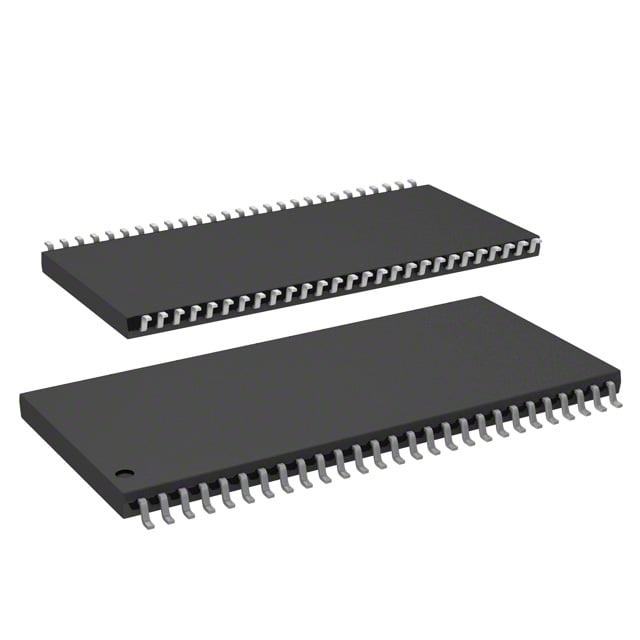
| Device Package | 54-TSOP II | Memory Format | DRAM | Technology | SDRAM | ||
|---|---|---|---|---|---|---|---|
| Memory Size | 128 Mbit | Access Time | 5.4 ns | Grade | Industrial | ||
| Clock Frequency | 143 MHz | Voltage | 3V ~ 3.6V | Memory Type | Volatile | ||
| Operating Temperature | -40°C ~ 85°C (TA) | Write Cycle Time Word Page | N/A | Packaging | 54-TSOP (0.400", 10.16mm Width) | ||
| Mounting Method | Volatile | Memory Interface | Parallel | Memory Organization | 8M x 16 | ||
| Moisture Sensitivity Level | 3 (168 Hours) | RoHS Compliance | ROHS3 Compliant | REACH Compliance | REACH Unaffected | ||
| Qualification | N/A | ECCN | EAR99 | HTS Code | 8542.32.0002 |
Overview of IS42S16800E-7TLI-TR – IC DRAM 128MBIT PAR 54TSOP II
The IS42S16800E-7TLI-TR is a 128 Mbit synchronous DRAM (SDRAM) organized as 8M × 16 with a parallel memory interface. It uses a pipelined, fully synchronous architecture with internal quad-bank operation to support high-speed data transfer and efficient row access/precharge hiding.
Designed for 3.3V memory systems (VDD/VDDQ = 3.3V) with an operational supply range of 3.0 V to 3.6 V and industrial temperature availability (–40°C to 85°C), this 54-pin TSOP II packaged device targets systems requiring reliable, mid‑density synchronous DRAM.
Key Features
- Memory Architecture 128 Mbit SDRAM organized as 8M × 16 with quad-bank internal configuration for parallel row/column operation and improved throughput.
- High-Speed Synchronous Operation Fully synchronous design with all signals referenced to the rising clock edge; supported clock frequency for the -7 speed grade is 143 MHz and access time from clock is 5.4 ns.
- Programmable Burst and CAS Programmable burst lengths (1, 2, 4, 8, full page) and selectable burst sequence (Sequential/Interleave). CAS latency is programmable to 2 or 3 clocks.
- Refresh and Power Modes Auto Refresh and Self Refresh supported with 4096 refresh cycles every 64 ms; includes power‑saving power‑down functionality.
- Interface and Signaling LVTTL-compatible interface supporting random column address access every clock cycle and burst read/write operations with burst termination commands.
- Supply and Packaging Designed for 3.3V VDD/VDDQ operation (supply range 3.0–3.6V) in a 54-pin TSOP II (0.400", 10.16 mm width) package for compact board-level placement.
- Industrial Temperature Range Rated for operation from –40°C to 85°C (TA), suitable for temperature-demanding environments.
Typical Applications
- Industrial Systems Use where industrial temperature range and reliable synchronous memory operation are required.
- Embedded Memory Subsystems Suitable as main or buffer memory in 3.3V synchronous memory designs that need mid-density DRAM.
- High-Speed Parallel Data Buffers Appropriate for designs leveraging pipelined SDRAM and burst access at up to 143 MHz clock rates.
Unique Advantages
- Synchronous Pipelined Architecture: Pipeline design with all signals registered to the clock edge enables predictable timing and high throughput.
- Flexible Burst Control: Programmable burst lengths and sequences allow tuning for sequential or interleaved access patterns to match system requirements.
- Selectable CAS Latency: CAS latency programmable to 2 or 3 clocks provides trade-offs between latency and clock rate for timing optimization.
- Industry-Grade Temperature Range: Operation from –40°C to 85°C supports deployment in harsher environments where extended temperature tolerance is needed.
- Standard 54‑TSOP II Package: Compact 54-pin TSOP II footprint simplifies board-level integration in space-constrained designs.
- 3.3V Supply Compatibility: Designed for 3.3V VDD/VDDQ with a supply range of 3.0–3.6V to align with common memory power rails.
Why Choose IS42S16800E-7TLI-TR?
The IS42S16800E-7TLI-TR combines a synchronous, pipelined SDRAM architecture with flexible burst and CAS programmability to deliver a reliable mid-density memory solution for 3.3V systems. Its quad-bank organization and supported 143 MHz clock rate enable efficient high-speed data transfers while maintaining industry-temperature operation.
This device is well suited for designers needing a compact 128 Mbit DRAM in a 54‑pin TSOP II package where predictable timing, refresh management, and selectable latency/burst modes are required for embedded and industrial memory subsystems.
Request a quote or submit an inquiry to receive pricing and availability information for the IS42S16800E-7TLI-TR.