IS42S16800E-7TL
| Part Description |
IC DRAM 128MBIT PAR 54TSOP II |
|---|---|
| Quantity | 42 Available (as of June 18, 2026) |

| Product Category | DRAM Memory |
|---|---|
| Manufacturer | Integrated Silicon Solution Inc |
| Manufacturing Status | Obsolete |
| Manufacturer Standard Lead Time | Contact Us |
| Datasheet |
Specifications & Environmental
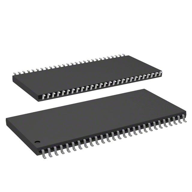
| Device Package | 54-TSOP II | Memory Format | DRAM | Technology | SDRAM | ||
|---|---|---|---|---|---|---|---|
| Memory Size | 128 Mbit | Access Time | 5.4 ns | Grade | Commercial | ||
| Clock Frequency | 143 MHz | Voltage | 3V ~ 3.6V | Memory Type | Volatile | ||
| Operating Temperature | 0°C ~ 70°C (TA) | Write Cycle Time Word Page | N/A | Packaging | 54-TSOP (0.400", 10.16mm Width) | ||
| Mounting Method | Volatile | Memory Interface | Parallel | Memory Organization | 8M x 16 | ||
| Moisture Sensitivity Level | 3 (168 Hours) | RoHS Compliance | ROHS3 Compliant | REACH Compliance | REACH Unaffected | ||
| Qualification | N/A | ECCN | EAR99 | HTS Code | 8542.32.0002 |
Overview of IS42S16800E-7TL – 128 Mbit SDRAM, 54‑TSOP II
The IS42S16800E-7TL is a 128 Mbit synchronous DRAM (SDRAM) device from Integrated Silicon Solution, Inc., organized as 8M × 16 with a parallel memory interface. It implements a quad‑bank, fully synchronous pipeline architecture with registered inputs and outputs referenced to the rising edge of the system clock.
Designed for high‑speed memory subsystems, the device provides programmable burst operations, internal bank management for hidden row access/precharge, and on‑chip refresh modes to support continuous data throughput and system memory needs.
Key Features
- Core Architecture Quad‑bank synchronous DRAM with internal bank structure to hide row access/precharge and support pipeline operation.
- Memory Organization 128 Mbit capacity configured as 8M × 16 (2M ×16 ×4 banks), offering parallel 16‑bit data access.
- Performance Supports a clock frequency up to 143 MHz for the -7 speed grade with CAS latency options of 2 or 3 clocks and an access time from clock of 5.4 ns at CL=3.
- Burst and Sequencing Programmable burst lengths (1, 2, 4, 8, full page) and selectable burst sequence (Sequential/Interleave) for flexible block transfers.
- Refresh and Power Management Auto Refresh and Self Refresh modes supported; 4096 refresh cycles every 64 ms are implemented for data integrity.
- Interface LVTTL signaling for control and data lines with a parallel memory interface.
- Power Operates from a 3.0 V to 3.6 V supply (VDD/VDDQ = 3.3V typical as specified in the datasheet).
- Package & Temperature Available in a 54‑pin TSOP II (0.400", 10.16 mm width) package and specified operating temperature range of 0°C to 70°C (TA).
Typical Applications
- System Memory Subsystems Provides 128 Mbit of synchronous, parallel memory for devices needing organized 8M × 16 storage and high‑speed access.
- High‑Speed Data Buffers Programmable burst lengths and internal bank architecture enable efficient block transfers and buffering in memory designs.
- Embedded Memory Modules TSOP II packaging and LVTTL interface allow integration into boards and modules that require a compact, parallel SDRAM solution.
Unique Advantages
- Deterministic Synchronous Operation: Fully synchronous, edge‑referenced signals and pipeline architecture simplify timing design and integration with clocked systems.
- Flexible Burst Transfer Options: Programmable burst length and sequence enable tuning for different data transfer patterns and throughput requirements.
- On‑Chip Refresh Support: Auto Refresh and Self Refresh modes with 4096 refresh cycles per 64 ms reduce external refresh management and help maintain data integrity.
- Compact Industry Package: 54‑pin TSOP II footprint (10.16 mm width) supports dense board layouts while providing standard pinout compatibility.
- Standard Voltage Range: 3.0 V to 3.6 V supply range (3.3 V typical) aligns with common memory system power rails.
Why Choose IS42S16800E-7TL?
The IS42S16800E-7TL positions itself as a pragmatic 128 Mbit SDRAM choice where synchronous, parallel memory with programmable burst behavior and internal bank management is required. Its 8M × 16 organization, support for up to 143 MHz clocking at the -7 speed grade, and on‑chip refresh features deliver a balanced combination of performance and system integration.
This device is suited for designs that need a compact TSOP II form factor, LVTTL interface, and standard 3.3 V memory operation, offering straightforward integration into established memory subsystems and embedded modules while relying on the documented timing and refresh characteristics in the datasheet.
If you require pricing, availability, or lead‑time information for the IS42S16800E-7TL, request a quote or contact the supplier sales channel to submit your requirements.