IS42S16800E-7TLI
| Part Description |
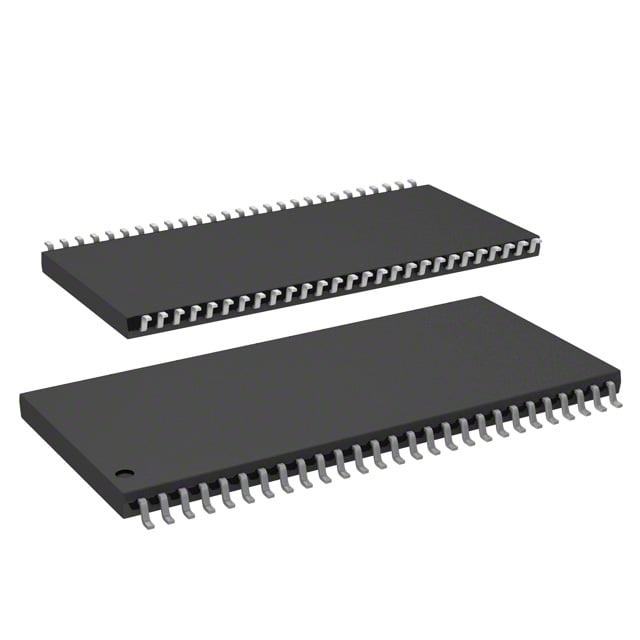
IC DRAM 128MBIT PAR 54TSOP II |
|---|---|
| Quantity | 100 Available (as of June 15, 2026) |

| Product Category | Memory |
|---|---|
| Manufacturer | Integrated Silicon Solution Inc |
| Manufacturing Status | Obsolete |
| Manufacturer Standard Lead Time | Contact Us |
| Datasheet |
Specifications & Environmental
| Device Package | 54-TSOP II | Memory Format | DRAM | Technology | SDRAM | ||
|---|---|---|---|---|---|---|---|
| Memory Size | 128 Mbit | Access Time | 5.4 ns | Grade | Industrial | ||
| Clock Frequency | 143 MHz | Voltage | 3V ~ 3.6V | Memory Type | Volatile | ||
| Operating Temperature | -40°C ~ 85°C (TA) | Write Cycle Time Word Page | N/A | Packaging | 54-TSOP (0.400", 10.16mm Width) | ||
| Mounting Method | Volatile | Memory Interface | Parallel | Memory Organization | 8M x 16 | ||
| Moisture Sensitivity Level | 3 (168 Hours) | RoHS Compliance | ROHS Compliant | REACH Compliance | REACH Unaffected | ||
| Qualification | N/A | ECCN | EAR99 | HTS Code | 8542.32.0002 |
Overview of IS42S16800E-7TLI – IC DRAM 128MBIT PAR 54TSOP II
The IS42S16800E-7TLI is a 128 Mbit synchronous DRAM (SDRAM) device organized as 8M × 16 and implemented in a quad‑bank architecture. It provides fully synchronous, pipeline operation with all signals referenced to the rising edge of the clock and is designed for 3.3 V memory systems.
Engineered for systems requiring high‑speed parallel SDRAM with industrial temperature availability (−40°C to 85°C), the device supports programmable burst lengths, selectable CAS latency, and power‑saving refresh modes for reliable memory performance in demanding environments.
Key Features
- Memory Core — 128 Mbit SDRAM organized as 8M × 16 (2M × 16 × 4 banks) with quad‑bank internal architecture for hidden row access/precharge.
- Performance — Clock frequency options include 143 MHz (−7 speed grade) with typical access time from clock of 5.4 ns at CAS latency = 3.
- Programmable Latency & Burst — Selectable CAS latency (2 or 3 clocks) and programmable burst lengths (1, 2, 4, 8, full page) with sequential or interleave burst sequence.
- Refresh & Power Modes — Supports Auto Refresh (CBR), Self Refresh, and power‑down; requires 4096 refresh cycles every 64 ms.
- Interface — LVTTL interface with parallel SDRAM signaling and random column address capability every clock cycle.
- Voltage & Supply — Designed for 3.3 V systems; operating supply range specified as 3.0 V to 3.6 V (VDD / VDDQ).
- Package & Mounting — Available in 54‑pin TSOP II (0.400", 10.16 mm width) package for board‑level mounting.
- Operating Temperature — Industrial temperature range: −40°C to 85°C (TA).
Typical Applications
- Industrial Systems — Memory for industrial control and instrumentation where the −40°C to 85°C temperature range is required.
- 3.3 V Memory Subsystems — Parallel SDRAM expansion in systems designed around 3.3 V VDD/VDDQ memory architectures.
- Embedded Memory Modules — High‑speed synchronous DRAM for embedded boards and modules requiring programmable burst and CAS options.
Unique Advantages
- High‑speed Synchronous Operation: Supports up to 143 MHz clock rate (−7 grade) with a 5.4 ns access time from clock for low‑latency data transfer.
- Flexible Data Transfer Modes: Programmable burst lengths and selectable burst sequence (sequential/interleave) allow tuning for different access patterns.
- Robust Refresh and Power Controls: Auto and self refresh modes plus power‑down support help manage power consumption and data retention.
- Industrial Temperature Availability: Specified operation from −40°C to 85°C for deployment in temperature‑challenging environments.
- Standard TSOP II Package: 54‑pin TSOP II footprint simplifies PCB integration for legacy and new designs using parallel SDRAM.
- 3.3 V System Compatibility: Designed for 3.3 V VDD/VDDQ systems with an operating range of 3.0 V to 3.6 V for broad system compatibility.
Why Choose IS42S16800E-7TLI?
The IS42S16800E-7TLI delivers a compact 128 Mbit SDRAM solution with synchronous, pipelined operation and quad‑bank organization to support high‑throughput parallel memory designs. Its programmable CAS latency and burst options, combined with industry‑rated temperature operation and standard TSOP II packaging, make it suitable for system designers seeking predictable, spec‑driven memory behavior.
This device is well suited for designs that require deterministic synchronous DRAM performance in 3.3 V memory systems and where industrial temperature range and standard packaging simplify integration and deployment.
If you need pricing, lead‑time, or volume availability, request a quote or contact sales to discuss your requirements and obtain a formal quotation.