IS42S16800E-7BL
| Part Description |
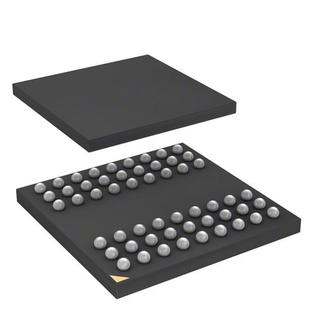
IC DRAM 128MBIT PAR 54TFBGA |
|---|---|
| Quantity | 545 Available (as of June 15, 2026) |

| Product Category | DRAM Memory |
|---|---|
| Manufacturer | Integrated Silicon Solution Inc |
| Manufacturing Status | Obsolete |
| Manufacturer Standard Lead Time | Contact Us |
| Datasheet |
Specifications & Environmental
| Device Package | 54-TFBGA (8x8) | Memory Format | DRAM | Technology | SDRAM | ||
|---|---|---|---|---|---|---|---|
| Memory Size | 128 Mbit | Access Time | 5.4 ns | Grade | Commercial | ||
| Clock Frequency | 143 MHz | Voltage | 3V ~ 3.6V | Memory Type | Volatile | ||
| Operating Temperature | 0°C ~ 70°C (TA) | Write Cycle Time Word Page | N/A | Packaging | 54-TFBGA | ||
| Mounting Method | Volatile | Memory Interface | Parallel | Memory Organization | 8M x 16 | ||
| Moisture Sensitivity Level | 3 (168 Hours) | RoHS Compliance | ROHS3 Compliant | REACH Compliance | REACH Unaffected | ||
| Qualification | N/A | ECCN | EAR99 | HTS Code | 8542.32.0002 |
Overview of IS42S16800E-7BL – IC DRAM 128MBIT PAR 54TFBGA
The IS42S16800E-7BL is a 128 Mbit synchronous DRAM organized as 8M × 16, implemented with a quad-bank, fully synchronous pipeline architecture. It is designed for 3.3 V memory systems and provides parallel SDRAM operation with programmable burst and latency settings.
Designed for systems that require low-latency, high-throughput parallel memory, the device delivers selectable CAS latency, burst lengths and sequences, and built-in refresh modes to support sustained data transfers and predictable timing behavior.
Key Features
- Memory Core 128 Mbit SDRAM organized as 8M × 16 with quad-bank architecture for internal row access/precharge hiding.
- Performance Clock frequency up to 143 MHz for the -7 speed grade with access time of 5.4 ns (CAS latency = 3).
- Programmable Timing & Burst Programmable CAS latency (2 or 3 clocks) and selectable burst lengths (1, 2, 4, 8, full page) with sequential or interleaved burst sequences.
- Interface Parallel memory interface with LVTTL I/O signaling; all signals referenced to the positive clock edge for fully synchronous operation.
- Refresh & Power Modes Auto Refresh and Self Refresh supported with 4096 refresh cycles every 64 ms; includes power-saving power-down mode.
- Power Operates from 3.0 V to 3.6 V supply (VDD/VDDQ nominal 3.3 V as specified in device overview).
- Package & Temperature 54-ball TF-BGA package (54-TFBGA, 8 × 8) and specified operating temperature range 0°C to 70°C (TA).
Typical Applications
- 3.3 V Synchronous Memory Systems Acts as main DRAM in system memory designs that require a parallel SDRAM interface and synchronous clocked operation.
- Embedded Platforms Provides burst read/write capability and programmable latency for embedded systems that need predictable memory timing.
- High-Speed Data Buffers Suitable for designs that require pipeline architecture and quad-bank access to support sustained data transfer operations.
Unique Advantages
- Selectable CAS Latency: Programmable CAS = 2 or 3 clocks enables trade-offs between throughput and latency to match system timing requirements.
- Flexible Burst Control: Burst lengths from 1 to full page and sequential/interleaved modes simplify burst-oriented transfers and memory controller integration.
- Quad-Bank Architecture: Internal bank structure helps hide row access/precharge time and supports efficient multi-access patterns.
- Synchronous Pipeline Design: All inputs and outputs are referenced to the positive clock edge, enabling consistent timing and easier system synchronization.
- Wide Supply Range: 3.0 V–3.6 V supply support with nominal 3.3 V operation accommodates typical 3.3 V memory system rails.
- Compact TF-BGA Package: 54-ball TF-BGA (8 × 8) package saves board area while providing the required ballout for parallel SDRAM integration.
Why Choose IS42S16800E-7BL?
The IS42S16800E-7BL combines a 128 Mbit SDRAM density with a fully synchronous, quad-bank pipeline architecture and programmable timing features to deliver predictable, low-latency parallel memory performance in 3.3 V systems. Its selectable CAS latency, flexible burst modes and built-in refresh capabilities make it appropriate for designs that require controlled timing and sustained data throughput.
This device is suited for engineers and procurement teams specifying parallel SDRAM in space-constrained board designs that require a 54-ball TF-BGA package and operation across the 0°C to 70°C commercial temperature range. Its feature set supports scalable integration into systems that rely on synchronous memory timing and burst-oriented transfers.
Request a quote or submit an inquiry for pricing and availability of IS42S16800E-7BL to get detailed lead time and ordering information.