IS42S16800E-75ETL
| Part Description |
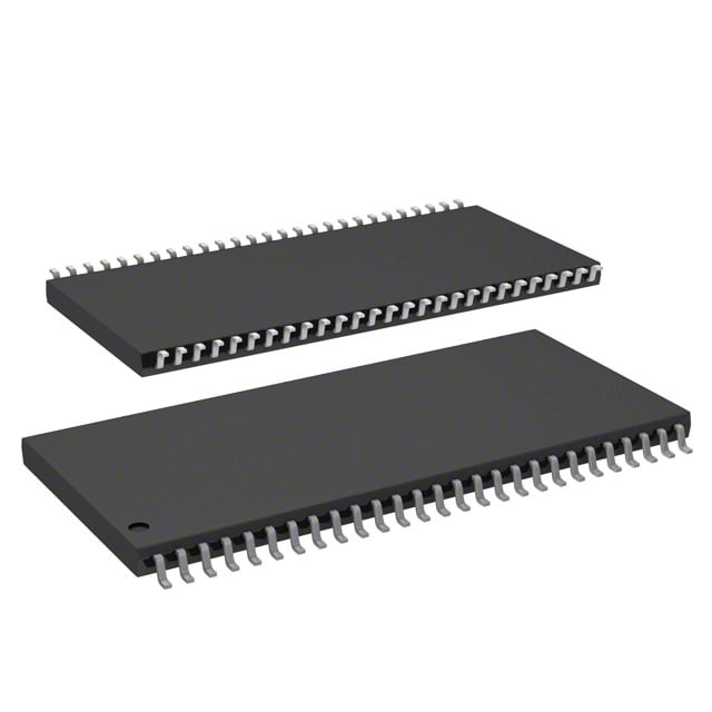
IC DRAM 128MBIT PAR 54TSOP II |
|---|---|
| Quantity | 658 Available (as of June 13, 2026) |

| Product Category | Memory |
|---|---|
| Manufacturer | Integrated Silicon Solution Inc |
| Manufacturing Status | Obsolete |
| Manufacturer Standard Lead Time | Contact Us |
| Datasheet |
Specifications & Environmental
| Device Package | 54-TSOP II | Memory Format | DRAM | Technology | SDRAM | ||
|---|---|---|---|---|---|---|---|
| Memory Size | 128 Mbit | Access Time | 5.4 ns | Grade | Commercial | ||
| Clock Frequency | 133 MHz | Voltage | 3V ~ 3.6V | Memory Type | Volatile | ||
| Operating Temperature | 0°C ~ 70°C (TA) | Write Cycle Time Word Page | N/A | Packaging | 54-TSOP (0.400", 10.16mm Width) | ||
| Mounting Method | Volatile | Memory Interface | Parallel | Memory Organization | 8M x 16 | ||
| Moisture Sensitivity Level | 3 (168 Hours) | RoHS Compliance | ROHS Compliant | REACH Compliance | REACH Unaffected | ||
| Qualification | N/A | ECCN | EAR99 | HTS Code | 8542.32.0002 |
Overview of IS42S16800E-75ETL – IC DRAM 128MBIT PAR 54TSOP II
The IS42S16800E-75ETL is a 128Mbit synchronous DRAM (SDRAM) organized as 8M × 16 with a parallel memory interface in a 54‑pin TSOP II package. The device implements a fully synchronous pipeline architecture with internal bank management and supports programmable burst operations and CAS latency options.
This device is intended for systems that require a 128Mbit parallel SDRAM solution with defined timing and refresh behavior, providing measured performance (133 MHz Clock/5.4 ns access time on the -75E option), programmable burst sequencing, and built‑in refresh and self‑refresh functions.
Key Features
- Memory Density & Organization — 128 Mbit density configured as 8M × 16 with quad-bank internal organization.
- Synchronous SDRAM Architecture — Fully synchronous operation with all inputs and outputs referenced to the rising clock edge and pipeline architecture for high-speed transfers.
- Clock & Timing (‑75E option) — Supports a 133 MHz clock frequency with an access time from clock of 5.4 ns (CAS latency = 2 for the -75E variant).
- Programmable Burst & CAS — Programmable burst lengths (1, 2, 4, 8, full page), sequential or interleave burst sequences, and selectable CAS latency (2 or 3 clocks as supported by device options).
- Refresh & Power Modes — Auto Refresh (CBR) and Self Refresh supported with 4096 refresh cycles every 64 ms; includes power‑down capability.
- Interface & I/O — LVTTL interface signaling and parallel memory interface for board‑level memory subsystems.
- Supply & Mounting — Specified supply range of 3.0 V to 3.6 V; standard 54‑pin TSOP (0.400", 10.16 mm width) TSOP II package for surface mounting.
- Operating Temperature — Commercial operating range of 0°C to 70°C (TA).
Typical Applications
- Embedded memory subsystems — Provides 128 Mbit of synchronous parallel DRAM capacity for designs requiring organized 8M × 16 memory.
- Board‑level memory expansion — Standard 54‑pin TSOP II package enables integration into PCBs for parallel SDRAM expansion.
- High‑throughput buffering — Programmable burst lengths and synchronous interface support burst read/write buffering at the specified clock and access timings.
Unique Advantages
- Deterministic synchronous timing — All signals referenced to the clock edge and pipeline architecture enable predictable timing behavior tied to the 133 MHz/5.4 ns specification for the -75E variant.
- Flexible data access — Programmable burst lengths and sequence options plus selectable CAS latency allow tuning for system timing and throughput.
- Refresh and power management — Auto Refresh and Self Refresh modes with defined refresh rate (4096 cycles/64 ms) simplify system refresh management and power control.
- Board-friendly package — 54‑pin TSOP II (10.16 mm width) offers a compact, surface‑mount package compatible with standard PCB assembly processes.
- Wide supply tolerance — Operates across a 3.0 V to 3.6 V supply range with device operation defined at 3.3 V in the datasheet.
Why Choose IC DRAM 128MBIT PAR 54TSOP II?
The IS42S16800E-75ETL delivers a compact, parallel 128Mbit SDRAM option with synchronous pipeline architecture, programmable burst/CAS options, and defined timing (133 MHz / 5.4 ns on the -75E part). Its combination of refresh management, LVTTL interface, and a standard 54‑pin TSOP II package makes it suitable for designs that require predictable, board‑level parallel memory with configurable access patterns.
This device is well suited for engineers specifying a commercial‑temperature parallel SDRAM solution where known timing, refresh behavior, and package footprint are required. Its feature set supports straightforward integration into memory subsystems that rely on synchronous, burst‑capable DRAM.
Request a quote or submit a request for pricing and availability to receive further commercial details and lead‑time information.