IS42S16800E-75EBL-TR
| Part Description |
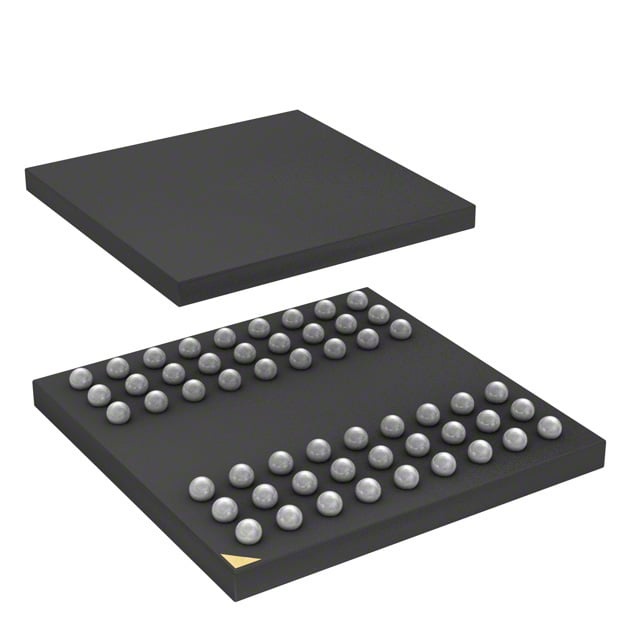
IC DRAM 128MBIT PAR 54TFBGA |
|---|---|
| Quantity | 653 Available (as of June 14, 2026) |

| Product Category | Memory |
|---|---|
| Manufacturer | Integrated Silicon Solution Inc |
| Manufacturing Status | Obsolete |
| Manufacturer Standard Lead Time | Contact Us |
| Datasheet |
Specifications & Environmental
| Device Package | 54-TFBGA (8x8) | Memory Format | DRAM | Technology | SDRAM | ||
|---|---|---|---|---|---|---|---|
| Memory Size | 128 Mbit | Access Time | 5.4 ns | Grade | Commercial | ||
| Clock Frequency | 133 MHz | Voltage | 3V ~ 3.6V | Memory Type | Volatile | ||
| Operating Temperature | 0°C ~ 70°C (TA) | Write Cycle Time Word Page | N/A | Packaging | 54-TFBGA | ||
| Mounting Method | Volatile | Memory Interface | Parallel | Memory Organization | 8M x 16 | ||
| Moisture Sensitivity Level | 3 (168 Hours) | RoHS Compliance | ROHS3 Compliant | REACH Compliance | REACH Unaffected | ||
| Qualification | N/A | ECCN | EAR99 | HTS Code | 8542.32.0002 |
Overview of IS42S16800E-75EBL-TR – 128Mbit Synchronous DRAM (54‑TFBGA)
The IS42S16800E-75EBL-TR is a 128Mbit synchronous DRAM (SDRAM) organized as 8M × 16 with a quad-bank architecture and pipeline operation. It is a fully synchronous, LVTTL‑interfaced parallel DRAM device designed for high‑speed data transfer within 3.3V memory systems.
Built for system memory applications that require low access latency and flexible burst control, this device provides programmable burst lengths and sequence modes together with auto- and self‑refresh capabilities for reliable operation in standard temperature environments.
Key Features
- Memory Architecture 128 Mbit SDRAM organized as 8M × 16 with internal quad‑bank configuration to support pipelined and interleaved operations.
- Clock and Timing –75E speed grade: 133 MHz clock frequency and 5.4 ns access time (CAS latency = 2 timing for the –75E grade).
- Programmable Burst and Latency Supports programmable burst lengths (1, 2, 4, 8, full page) and programmable burst sequence (Sequential/Interleave); CAS latency programmable to 2 or 3 clocks.
- Refresh and Power Modes Auto Refresh (CBR) and Self Refresh supported with 4096 refresh cycles every 64 ms; power‑saving power‑down mode available.
- Interface and Signaling LVTTL input/output signaling with a parallel memory interface and fully synchronous inputs/outputs referenced to the rising clock edge.
- Power Supply Rated for 3.0 V to 3.6 V operation with VDD/VDDQ 3.3 V nominal as indicated in device documentation.
- Package and Mounting 54‑ball Thin Fine‑pitch BGA (54‑TFBGA, 8×8) package suitable for space‑constrained board layouts; device is volatile DRAM.
- Operating Temperature Specified for commercial operation from 0°C to 70°C (TA).
- Row/Column Performance Random column address capability every clock cycle and internal bank operation to hide row access/precharge latency.
Typical Applications
- Memory subsystems Integration as synchronous DRAM in 3.3V memory systems requiring quad‑bank, high‑throughput buffering.
- High‑speed buffering Use where pipelined SDRAM transfers and low access latency (5.4 ns at –75E) are needed for transient data storage.
- System modules Onboard DRAM for modules or subsystems that require programmable burst control and LVTTL interfacing.
Unique Advantages
- Synchronous pipeline architecture: Enables high‑speed data transfer with all signals referenced to the rising clock edge for predictable timing.
- Flexible burst control: Programmable burst lengths and sequence modes simplify matching memory transfers to system access patterns.
- Low latency performance: –75E timing provides a 133 MHz clock option and 5.4 ns access time for responsive memory access.
- Refresh and power management: Auto and self‑refresh modes with defined refresh cycle requirements help maintain data integrity while supporting power saving.
- Compact TF‑BGA package: 54‑TFBGA (8×8) ballout minimizes board area for space‑constrained designs.
- Standard voltage compatibility: 3.0 V to 3.6 V range with 3.3 V nominal VDD/VDDQ conforms to common 3.3V memory system designs.
Why Choose IS42S16800E-75EBL-TR?
The IS42S16800E-75EBL-TR delivers a compact, fully synchronous 128 Mbit SDRAM solution with programmable burst control, low access latency, and quad‑bank internal architecture for pipelined operation. Its combination of LVTTL interfacing, defined timing for the –75E speed grade, and standard 3.3V nominal operation make it suitable for memory subsystems that demand predictable timing and efficient burst transfers.
This device is appropriate for designers seeking a verified SDRAM component in a small 54‑TFBGA footprint, offering refresh management and power‑down options to balance performance and power. Its documented timing and operating conditions provide the deterministic behavior required for system integration and long‑term support.
Request a quote or submit an inquiry to obtain pricing, availability, and ordering information for the IS42S16800E-75EBL-TR.