IS42S16800E-7BL-TR
| Part Description |
IC DRAM 128MBIT PAR 54TFBGA |
|---|---|
| Quantity | 850 Available (as of June 15, 2026) |

| Product Category | Memory |
|---|---|
| Manufacturer | Integrated Silicon Solution Inc |
| Manufacturing Status | Obsolete |
| Manufacturer Standard Lead Time | Contact Us |
| Datasheet |
Specifications & Environmental
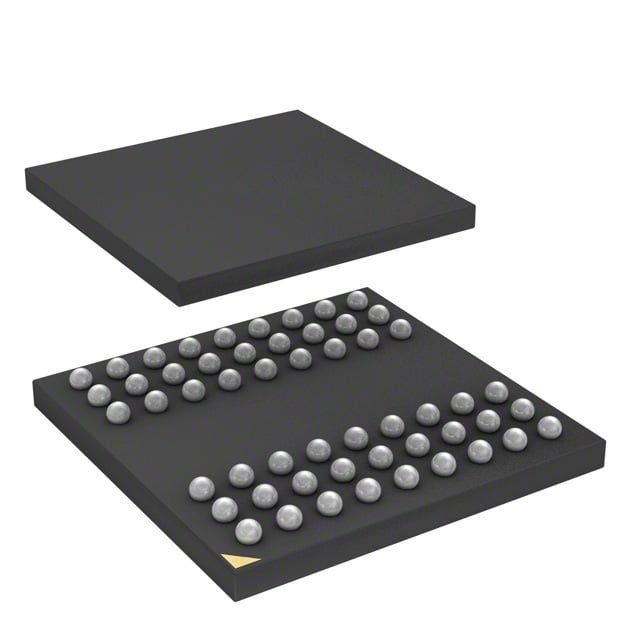
| Device Package | 54-TFBGA (8x8) | Memory Format | DRAM | Technology | SDRAM | ||
|---|---|---|---|---|---|---|---|
| Memory Size | 128 Mbit | Access Time | 5.4 ns | Grade | Commercial | ||
| Clock Frequency | 143 MHz | Voltage | 3V ~ 3.6V | Memory Type | Volatile | ||
| Operating Temperature | 0°C ~ 70°C (TA) | Write Cycle Time Word Page | N/A | Packaging | 54-TFBGA | ||
| Mounting Method | Volatile | Memory Interface | Parallel | Memory Organization | 8M x 16 | ||
| Moisture Sensitivity Level | 3 (168 Hours) | RoHS Compliance | ROHS3 Compliant | REACH Compliance | REACH Unaffected | ||
| Qualification | N/A | ECCN | EAR99 | HTS Code | 8542.32.0002 |
Overview of IS42S16800E-7BL-TR – IC DRAM 128MBIT PAR 54TFBGA
The IS42S16800E-7BL-TR is a 128Mbit synchronous DRAM organized as 8M × 16 with a parallel memory interface in a 54-ball TF‑BGA (8×8) package. It uses a fully synchronous pipeline architecture with internal bank management to optimize high-speed data transfer.
Designed for systems that require compact, 128Mbit SDRAM footprint with programmable burst modes and low-latency operation, this device targets applications requiring predictable timing, 3.3V memory operation, and a compact TF‑BGA package for surface-mount assembly.
Key Features
- Memory Organization & Capacity — 128 Mbit capacity configured as 8M × 16, internally arranged as quad banks for concurrent access and improved throughput.
- Synchronous SDRAM Architecture — Fully synchronous operation with all signals referenced to the positive clock edge; pipeline architecture for high-speed transfer.
- Speed & Timing — Clock frequency up to 143 MHz for the -7 grade; typical access time from clock of 5.4 ns (CAS latency = 3). Programmable CAS latency options of 2 or 3 clocks.
- Burst & Access Modes — Programmable burst length (1, 2, 4, 8, full page) and burst sequence (Sequential/Interleave); supports burst read/write and burst read/single write with burst termination commands.
- Refresh & Power Modes — Auto Refresh and Self Refresh support with 4096 refresh cycles every 64 ms; includes power‑down capability for power savings.
- Power Supply — Operates across a supply range of 3.0 V to 3.6 V; datasheet specifies VDD and VDDQ at 3.3 V for standard operation.
- Interface & Logic — LVTTL-compatible interface signals; random column address capability every clock cycle for flexible access patterns.
- Package & Temperature — 54-TFBGA (8×8) ball grid package suitable for surface-mount assembly; specified operating temperature 0°C to 70°C (TA). Datasheet notes industrial temperature availability for the family.
Typical Applications
- Embedded systems memory — Provides 128Mbit synchronous DRAM capacity and predictable timing for embedded controllers and board-level system memory.
- High-speed buffering — Pipeline architecture and internal banking make it suitable for data buffering and temporary storage in systems requiring fast burst transfers.
- Consumer and industrial electronics — 3.3V operation and compact 54-ball TF‑BGA package enable use in space-constrained designs with standard memory interfaces.
Unique Advantages
- Deterministic timing options — Programmable CAS latency (2 or 3) and defined access times (5.4 ns at CL=3) help designers meet tight timing budgets.
- Flexible burst control — Multiple programmable burst lengths and sequence modes allow tuning of transfer patterns to system requirements.
- Compact surface-mount package — 54‑ball TF‑BGA (8×8) reduces board area and supports modern SMT assembly processes.
- Standard 3.3V supply — Operates within a 3.0–3.6 V range with VDD/VDDQ = 3.3 V, matching common system power rails for straightforward integration.
- Built-in refresh and power modes — Auto Refresh, Self Refresh, and power‑down modes simplify power management and data integrity across operating conditions.
- Quad-bank organization — Internal bank architecture hides row access/precharge latency to improve effective throughput for interleaved access patterns.
Why Choose IC DRAM 128MBIT PAR 54TFBGA?
IS42S16800E-7BL-TR delivers a compact 128Mbit SDRAM solution with synchronous, pipeline architecture and programmable timing features to support designs that require predictable low-latency memory access. Its 8M × 16 organization, burst flexibility, and quad-bank structure provide designers with the tools to optimize throughput and memory efficiency.
This part is suited to designers targeting systems that run on 3.3V rails and need a small TF‑BGA footprint while maintaining synchronous SDRAM performance. The device family’s refresh and power modes, combined with documented timing parameters, support long-term design stability and predictable integration into board-level memory subsystems.
Request a quote or submit an inquiry to receive pricing and availability details for IS42S16800E-7BL-TR.