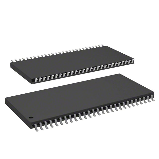
IS42S81600E-7TL-TR
| Part Description |
IC DRAM 128MBIT PAR 54TSOP II |
|---|---|
| Quantity | 1,266 Available (as of June 18, 2026) |

| Product Category | DRAM Memory |
|---|---|
| Manufacturer | Integrated Silicon Solution Inc |
| Manufacturing Status | Obsolete |
| Manufacturer Standard Lead Time | Contact Us |
| Datasheet |
Specifications & Environmental
| Device Package | 54-TSOP II | Memory Format | DRAM | Technology | SDRAM | ||
|---|---|---|---|---|---|---|---|
| Memory Size | 128 Mbit | Access Time | 5.4 ns | Grade | Commercial | ||
| Clock Frequency | 143 MHz | Voltage | 3V ~ 3.6V | Memory Type | Volatile | ||
| Operating Temperature | 0°C ~ 70°C (TA) | Write Cycle Time Word Page | N/A | Packaging | 54-TSOP (0.400", 10.16mm Width) | ||
| Mounting Method | Volatile | Memory Interface | Parallel | Memory Organization | 16M x 8 | ||
| Moisture Sensitivity Level | 3 (168 Hours) | RoHS Compliance | ROHS Compliant | REACH Compliance | REACH Unaffected | ||
| Qualification | N/A | ECCN | EAR99 | HTS Code | 8542.32.0002 |
Overview of IS42S81600E-7TL-TR – IC DRAM 128MBIT PAR 54TSOP II
The IS42S81600E-7TL-TR is a 128 Mbit synchronous DRAM (SDRAM) device organized as 16M × 8 with a parallel memory interface in a 54-pin TSOP II package. It implements a quad-bank, fully synchronous architecture with pipeline operation and is offered by Integrated Silicon Solution, Inc (ISSI).
Designed for 3.3 V-class memory systems, this device supports a 143 MHz clock timing grade (–7), CAS latency options and programmable burst operations, making it suitable for applications requiring deterministic, clocked DRAM performance in a compact TSOP footprint.
Key Features
- Core / Architecture Fully synchronous SDRAM with internal quad-bank architecture and pipeline operation; all signals are registered on the rising edge of CLK.
- Memory Organization 128 Mbit capacity configured as 16M × 8; internal banks and row/column organization support high-density memory mapping.
- Performance –7 timing grade supports a 143 MHz clock with CAS latency = 3 and an access time from clock of 5.4 ns.
- Programmable Burst & Timing Programmable burst lengths (1, 2, 4, 8, full page) and programmable burst sequence (sequential/interleave); CAS latency selectable (2 or 3 clocks).
- Refresh & Power Modes Auto Refresh and Self Refresh supported; 4096 refresh cycles every 64 ms and power-down/power-saving modes described in device documentation.
- Interface LVTTL-compatible inputs with a parallel memory interface and random column address capability every clock cycle.
- Power Designed for 3.0 V to 3.6 V supply range (device specified for 3.3 V VDD / VDDQ operation in datasheet).
- Package & Mounting 54-pin TSOP II package (0.400" / 10.16 mm width) for compact board-level mounting.
- Operating Temperature Specified operating ambient temperature range: 0°C to 70°C (TA).
Typical Applications
- Memory Subsystems Provides 128 Mbit parallel SDRAM capacity (16M × 8) for systems requiring clocked, synchronous DRAM in a TSOP II package.
- Embedded Systems Suitable where a 3.3 V parallel SDRAM device with programmable burst operations and CAS latency options is required.
- Compact Board Designs 54-pin TSOP II packaging supports dense board-level integration where package footprint and parallel memory interface are design drivers.
Unique Advantages
- Clocked, Deterministic Operation: Fully synchronous design with signals referenced to the positive clock edge simplifies timing analysis and integration into clocked memory subsystems.
- Flexible Data Transfer Modes: Programmable burst lengths and sequences plus burst read/write modes enable tuning for sequential and random access patterns.
- Selectable CAS Latency: CAS latency options (2 or 3 clocks) allow trade-offs between latency and operating frequency to match system timing requirements.
- Integrated Refresh Management: Auto Refresh and Self Refresh support with 4096 refresh cycles per 64 ms reduces external refresh overhead and supports low-power states.
- Compact TSOP II Package: 54-pin TSOP II (10.16 mm width) enables denser memory placement on space-constrained PCBs.
- 3.3 V-Class Compatibility: Device operation aligned to 3.3 V VDD/VDDQ with specified supply range 3.0 V to 3.6 V for common 3.3 V memory system integration.
Why Choose IC DRAM 128MBIT PAR 54TSOP II?
The IS42S81600E-7TL-TR combines a 128 Mbit SDRAM capacity, synchronous quad-bank architecture and a small 54-pin TSOP II package to address designs that require a compact, clocked parallel memory solution at 3.3 V. Its –7 timing grade (143 MHz) with CAS latency options and programmable burst functionality provides predictable timing and flexible data transfer modes for system-level tuning.
Backed by ISSI product documentation and datasheet details, this device is suited for engineers specifying parallel SDRAM memory on constrained PCBs who need verifiable timing, refresh control and package-level compatibility with 54-pin TSOP II mounting.
Request a quote or submit a request for pricing and availability to obtain lead-time and ordering information for IS42S81600E-7TL-TR.