
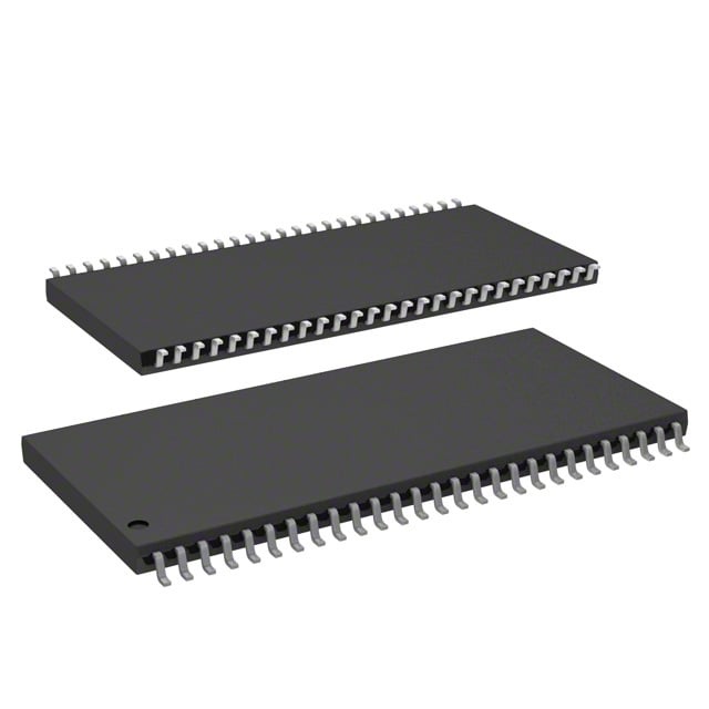
IS42S81600E-7TLI
| Part Description |
IC DRAM 128MBIT PAR 54TSOP II |
|---|---|
| Quantity | 216 Available (as of June 15, 2026) |
| Product Category | Memory |
|---|---|
| Manufacturer | Integrated Silicon Solution Inc |
| Manufacturing Status | Obsolete |
| Manufacturer Standard Lead Time | Contact Us |
| Datasheet |
Specifications & Environmental
| Device Package | 54-TSOP II | Memory Format | DRAM | Technology | SDRAM | ||
|---|---|---|---|---|---|---|---|
| Memory Size | 128 Mbit | Access Time | 5.4 ns | Grade | Industrial | ||
| Clock Frequency | 143 MHz | Voltage | 3V ~ 3.6V | Memory Type | Volatile | ||
| Operating Temperature | -40°C ~ 85°C (TA) | Write Cycle Time Word Page | N/A | Packaging | 54-TSOP (0.400", 10.16mm Width) | ||
| Mounting Method | Volatile | Memory Interface | Parallel | Memory Organization | 16M x 8 | ||
| Moisture Sensitivity Level | 3 (168 Hours) | RoHS Compliance | ROHS3 Compliant | REACH Compliance | REACH Unaffected | ||
| Qualification | N/A | ECCN | EAR99 | HTS Code | 8542.32.0002 |
Overview of IS42S81600E-7TLI – IC DRAM 128Mbit Parallel SDRAM, 54-TSOP II
The IS42S81600E-7TLI is a 128Mbit synchronous DRAM organized as 16M × 8 with a quad-bank, pipelined architecture for high-speed, clocked memory operations. It is designed for synchronous, parallel memory subsystems requiring programmable burst modes, internal bank management, and standard LVTTL signaling.
This device targets applications and systems that require a compact 54-pin TSOP II package, operation across an industrial temperature range (-40°C to 85°C), and a nominal 3.3V VDD memory environment with a supply range of 3.0V to 3.6V. The -7 speed grade supports a 143 MHz clock with CAS latency options for low access-time operation.
Key Features
- Memory Core 128 Mbit SDRAM organized as 16M × 8 with internal quad-bank architecture enabling hidden row access and precharge for efficient pipelined operation.
- Performance -7 speed grade supports a 143 MHz clock frequency and CAS latency options (2 or 3 clocks); access times from clock as low as 5.4 ns for CAS = 3 in this grade.
- Burst and Access Modes Programmable burst lengths (1, 2, 4, 8, full page) and selectable burst sequences (sequential or interleave) with burst read/write and burst read/single write capabilities; burst termination via stop or precharge commands.
- Refresh and Power Management Auto Refresh and Self Refresh support with 4096 refresh cycles every 64 ms; includes a power-down mode for reduced power consumption during idle periods.
- Interface Fully synchronous LVTTL interface with all signals referenced to the rising edge of CLK; random column addressing every clock cycle for high throughput.
- Voltage and Supply Designed for 3.3V VDD (operating supply range 3.0V–3.6V) with matched VDDQ, suitable for standard 3.3V memory systems.
- Package and Mounting Supplied in a 54-pin TSOP II package (0.400" / 10.16 mm width) for compact PCB footprint and surface-mount assembly.
- Temperature Range Industrial temperature availability with operating range from -40°C to 85°C (TA).
Typical Applications
- Industrial Memory Subsystems Use where -40°C to 85°C operation and predictable refresh behavior are required for system stability.
- High‑Speed Buffering Suitable for designs needing synchronous, pipelined DRAM buffering with 143 MHz clock capability and low CAS latency.
- Compact PCB Designs 54-TSOP II package fits space-constrained boards that require a parallel DRAM interface and standard 3.3V supply.
Unique Advantages
- Deterministic Synchronous Operation: All inputs and outputs are registered to the positive clock edge, enabling timing predictability in synchronous memory systems.
- Flexible Burst Control: Multiple programmable burst lengths and sequences allow designers to optimize throughput and latency for varied access patterns.
- Low Access-Time Performance: -7 grade provides a 143 MHz clock with access times from clock as low as 5.4 ns (CAS = 3), supporting time-critical read operations.
- Industrial Temperature Support: Rated for -40°C to 85°C, making the device suitable for harsher operating environments where temperature resilience is required.
- Compact, Surface‑Mount Package: 54-pin TSOP II (10.16 mm width) reduces board area while retaining a parallel DRAM interface for legacy and contemporary designs.
- Standard 3.3V Memory System Compatibility: Designed for 3.3V VDD systems with a 3.0–3.6V supply range, simplifying integration into existing 3.3V memory architectures.
Why Choose IS42S81600E-7TLI?
The IS42S81600E-7TLI combines a compact 54-TSOP II footprint with a 128Mbit, quad-bank synchronous DRAM architecture to deliver predictable, high-speed memory performance for systems that require programmable burst modes, internal bank management, and LVTTL signaling. Its -7 speed grade, 143 MHz operation, and low access times make it suitable for designs with tight timing requirements.
This device is intended for designers and procurement teams seeking a reliable, industrial-temperature-capable SDRAM that integrates into 3.3V memory subsystems while offering flexible refresh and power-management features such as Auto Refresh, Self Refresh, and power-down modes for energy-conscious designs.
Request a quote or submit an inquiry to receive pricing and availability information for IS42S81600E-7TLI and to discuss how this 128 Mbit SDRAM can be integrated into your memory subsystem designs.


