IS43DR16160A-25EBL
| Part Description |
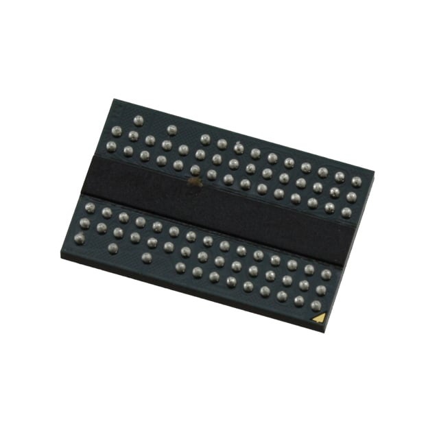
IC DRAM 256MBIT PAR 84TWBGA |
|---|---|
| Quantity | 1,451 Available (as of June 15, 2026) |

| Product Category | Memory |
|---|---|
| Manufacturer | Integrated Silicon Solution Inc |
| Manufacturing Status | Obsolete |
| Manufacturer Standard Lead Time | Contact Us |
| Datasheet |
Specifications & Environmental
| Device Package | 84-TWBGA (8x12.5) | Memory Format | DRAM | Technology | SDRAM - DDR2 | ||
|---|---|---|---|---|---|---|---|
| Memory Size | 256 Mbit | Access Time | 400 ns | Grade | Commercial | ||
| Clock Frequency | 400 MHz | Voltage | 1.7V ~ 1.9V | Memory Type | Volatile | ||
| Operating Temperature | 0°C ~ 70°C (TA) | Write Cycle Time Word Page | 15 ns | Packaging | 84-TFBGA | ||
| Mounting Method | Volatile | Memory Interface | Parallel | Memory Organization | 16M x 16 | ||
| Moisture Sensitivity Level | 3 (168 Hours) | RoHS Compliance | ROHS3 Compliant | REACH Compliance | REACH Unaffected | ||
| Qualification | N/A | ECCN | EAR99 | HTS Code | 8542.32.0024 |
Overview of IS43DR16160A-25EBL – IC DRAM 256MBIT PAR 84TWBGA
The IS43DR16160A-25EBL is a 256 Mbit DDR2 SDRAM device organized as 16M × 16 with a parallel memory interface. It implements a double-data-rate architecture and on-chip timing features to support high-speed synchronous memory operation.
This device is intended for designs that require a 256 Mbit volatile DRAM with programmable timing options, flexible drive-strength and on-die termination, and a compact 84-ball WBGA package.
Key Features
- Core Architecture Double data rate (DDR2) interface with 4-bit prefetch architecture and an on-chip DLL to align DQ and DQS transitions with CK.
- Memory Organization 256 Mbit density organized as 16M × 16 with 4 internal banks for concurrent operation.
- Timing & Performance Programmable CAS latency (CL = 3, 4, 5, 6) and programmable additive latency (AL = 0–5). Write latency equals read latency minus 1 tCK; programmable burst lengths of 4 or 8. Specified clock frequency: 400 MHz; write cycle time (word page) 15 ns; access time 400 ns.
- Signal & I/O Differential data strobe (DQS / DQS¯) and JEDEC-standard 1.8 V I/O (SSTL_18-compatible). Adjustable data-output drive strength and on-die termination (ODT) supported.
- Power Supply voltage range 1.7 V to 1.9 V for core and I/O (VDD = 1.8 V ±0.1 V, VDDQ = 1.8 V ±0.1 V).
- Package & Temperature 84-ball WBGA package (84-TWBGA, 8 mm × 12.5 mm) with an ambient operating temperature range of 0°C to 70°C (TA).
- System Reliability Built-in features for timing alignment and drive-strength control to help optimize signal integrity in synchronous parallel memory subsystems.
Typical Applications
- Parallel memory subsystems Used as a 256 Mbit DDR2 DRAM device in parallel memory designs that require programmable timing and ODT.
- High-speed buffering Provides synchronous DDR2 buffering where a 16M × 16 organization and programmable burst lengths are required.
- Compact board-level implementations Fits designs that need a small-footprint 84-ball WBGA memory package with 1.8 V supply requirements.
Unique Advantages
- Double-Data-Rate Architecture: Two data transfers per clock cycle via DDR2 and a 4-bit prefetch to maximize data throughput within the specified 400 MHz clock.
- Flexible Latency & Burst Control: Programmable CAS latencies (3–6), additive latency options, and burst lengths of 4 or 8 let designers tune performance for system timing and throughput.
- Signal Integrity Controls: Adjustable output drive strength and on-die termination (ODT) simplify board-level signal integrity management for high-speed operation.
- Compact WBGA Package: 84-ball WBGA (8 × 12.5 mm) provides a compact footprint for space-constrained designs while maintaining a 16-bit data width.
- Low-Voltage Operation: Narrow VDD/VDDQ range (1.7 V–1.9 V) aligned to 1.8 V JEDEC standards for consistent power and I/O behavior.
Why Choose IS43DR16160A-25EBL?
The IS43DR16160A-25EBL combines DDR2 double-data-rate architecture, programmable timing, and on-die signal management features in a compact 84-ball WBGA package. Its 16M × 16 organization and support for multiple CAS and additive latency settings make it suitable for designs that need configurable synchronous DRAM performance.
This device is appropriate for systems that require a 256 Mbit volatile memory element with controlled I/O characteristics, ODT support, and 1.8 V operation. The combination of timing flexibility and package density helps designers optimize board area, signal integrity, and memory timing for targeted system requirements.
Request a quote or submit an inquiry for IS43DR16160A-25EBL to obtain pricing, availability, and lead-time information for your next design.