
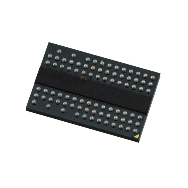
IS43DR16320D-25DBI-TR
| Part Description |
IC DRAM 512MBIT PAR 84TWBGA |
|---|---|
| Quantity | 478 Available (as of June 15, 2026) |
| Product Category | Memory |
|---|---|
| Manufacturer | Integrated Silicon Solution Inc |
| Manufacturing Status | Obsolete |
| Manufacturer Standard Lead Time | Contact Us |
| Datasheet |
Specifications & Environmental
| Device Package | 84-TWBGA (8x12.5) | Memory Format | DRAM | Technology | SDRAM - DDR2 | ||
|---|---|---|---|---|---|---|---|
| Memory Size | 512 Mbit | Access Time | 400 ps | Grade | Industrial | ||
| Clock Frequency | 400 MHz | Voltage | 1.7V ~ 1.9V | Memory Type | Volatile | ||
| Operating Temperature | -40°C ~ 85°C (TA) | Write Cycle Time Word Page | 15 ns | Packaging | 84-TFBGA | ||
| Mounting Method | Volatile | Memory Interface | Parallel | Memory Organization | 32M x 16 | ||
| Moisture Sensitivity Level | 3 (168 Hours) | RoHS Compliance | ROHS Compliant | REACH Compliance | REACH Unaffected | ||
| Qualification | N/A | ECCN | EAR99 | HTS Code | 8542.32.0028 |
Overview of IS43DR16320D-25DBI-TR – IC DRAM 512MBIT PAR 84TWBGA
The IS43DR16320D-25DBI-TR is a 512 Mbit DDR2 SDRAM device configured as 32M × 16 with a parallel memory interface. It implements a double-data-rate architecture with a 4n-prefetch and is designed for high-speed memory applications requiring standard DDR2 signaling.
Key attributes include a 400 MHz clock capability, JEDEC‑compatible 1.8 V I/O signaling, on‑chip DLL and differential DQS support, and an 84‑ball WBGA package for compact board-level integration.
Key Features
- Memory Architecture 512 Mbit DDR2 SDRAM organized as 32M × 16 with 4 internal banks and a 4‑bit prefetch architecture for double‑data‑rate transfers.
- High‑speed Operation Supports a 400 MHz clock frequency and timing options including programmable CAS latencies (CL = 3, 4, 5, 6) and selectable burst lengths of 4 or 8.
- Signal and Timing Differential data strobe (DQS/ DQS̄) and on‑chip DLL align DQ/DQS transitions with CK; write latency = read latency − 1 tCK for predictable timing behavior.
- Power and I/O VDD/VDDQ = 1.8 V ±0.1 V (specified operating supply range 1.7 V to 1.9 V) with JEDEC standard 1.8 V I/O (SSTL_18‑compatible) and adjustable data‑output drive strength.
- On‑Die Termination Integrated ODT reduces external termination requirements and simplifies signal integrity management on high‑speed buses.
- Package 84‑ball WBGA (84‑TWBGA) package, footprint 8 mm × 12.5 mm, suitable for space‑constrained PCB layouts.
- Operating Temperature Ambient operating range −40 °C to 85 °C as specified for TA.
- Other Timing Characteristics Key timing parameters published for the -25 speed grade include tRCD = 12.5 ns, tRP = 12.5 ns and available tCK options down to 2.5 ns at selected CL settings.
Typical Applications
- Embedded memory subsystems Provides a compact DDR2 memory option for embedded platforms requiring 512 Mbit density and parallel DDR2 interface.
- Networking and communications Suitable for buffering and packet memory functions where DDR2 performance and standard 1.8 V I/O are required.
- Industrial controllers Rated for ambient operation from −40 °C to 85 °C, appropriate for industrial‑temperature systems needing DDR2 SDRAM.
Unique Advantages
- Standard DDR2 signaling: JEDEC‑compatible 1.8 V I/O and differential DQS support ensure predictable integration with DDR2 memory interfaces.
- Flexible timing: Programmable CAS latencies, additive latency options and selectable burst lengths let designers tune performance to system requirements.
- On‑chip features that simplify design: On‑die termination and an on‑chip DLL reduce external component count for signal integrity and timing control.
- Compact WBGA package: 84‑ball WBGA (8 mm × 12.5 mm) provides a small footprint for space‑constrained PCB designs.
- Wide supply tolerance: Specified VDD/VDDQ range of 1.7 V to 1.9 V accommodates typical DDR2 power rails with tight margin control.
Why Choose IS43DR16320D-25DBI-TR?
The IS43DR16320D-25DBI-TR delivers a standards‑based DDR2 memory solution with 512 Mbit density, programmable timing options and integrated on‑chip features that reduce external BOM and simplify high‑speed design. Its 32M × 16 organization, differential DQS, and on‑die termination make it suitable for designs where predictable DDR2 timing and signal integrity are required.
This device is well suited to engineers designing embedded platforms, networking equipment, and industrial controllers that require compact, JEDEC‑compatible DDR2 memory with defined operating temperature and supply ranges.
Request a quote or submit an inquiry to receive pricing, lead‑time and availability information for the IS43DR16320D-25DBI-TR.


