IS43R86400E-5BI
| Part Description |
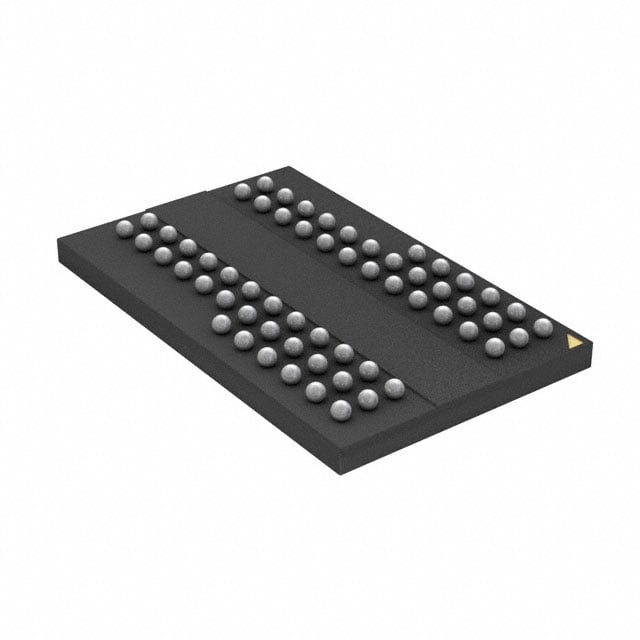
IC DRAM 512MBIT PAR 60TFBGA |
|---|---|
| Quantity | 606 Available (as of June 17, 2026) |
| Product Category | DRAM Memory |
|---|---|
| Manufacturer | Integrated Silicon Solution Inc |
| Manufacturing Status | Obsolete |
| Manufacturer Standard Lead Time | Contact Us |
| Datasheet |
Specifications & Environmental
| Device Package | 60-TFBGA (8x13) | Memory Format | DRAM | Technology | SDRAM - DDR | ||
|---|---|---|---|---|---|---|---|
| Memory Size | 512 Mbit | Access Time | 700 ps | Grade | Industrial | ||
| Clock Frequency | 200 MHz | Voltage | 2.3V ~ 2.7V | Memory Type | Volatile | ||
| Operating Temperature | -40°C ~ 85°C (TA) | Write Cycle Time Word Page | 15 ns | Packaging | 60-TFBGA | ||
| Mounting Method | Volatile | Memory Interface | Parallel | Memory Organization | 64M x 8 | ||
| Moisture Sensitivity Level | 3 (168 Hours) | RoHS Compliance | ROHS3 Compliant | REACH Compliance | REACH Unaffected | ||
| Qualification | N/A | ECCN | OBSOLETE | HTS Code | N/A |
Overview of IS43R86400E-5BI – 512Mbit DDR SDRAM, 60‑TFBGA
The IS43R86400E-5BI is a 512‑Mbit DDR SDRAM organized as 64M × 8 that uses a pipelined, double‑data‑rate architecture to deliver high‑speed burst transfers. The device implements four internal banks and supports programmable burst length and CAS latency to accommodate a range of memory access patterns.
Designed for systems requiring high‑speed volatile memory, the component provides SSTL_2 compatible I/O, differential clock inputs and a 60‑TFBGA (8×13) package with an industrial operating temperature range of −40°C to 85°C.
Key Features
- Core / Architecture 512 Mbit DDR SDRAM organized as 64M × 8 with four internal banks and pipelined operation for continuous read/write burst access.
- Performance Double‑data‑rate operation (two data transfers per clock cycle) with a clock frequency up to 200 MHz for the -5 speed grade and an access time of 700 ps.
- Interface & Timing SSTL_2 compatible I/O, differential clock inputs (CK and CK̄), data strobe (DQS) transmitted/received with data, DLL alignment of DQ/DQS to CK, burst lengths 2/4/8, and programmable CAS latency options of 2, 2.5 and 3.
- Read/Write Behavior DQS is edge‑aligned with data for READs and centre‑aligned with data for WRITEs; commands register on positive CK edges and data/mask are referenced to both edges of DQS.
- Refresh & Power Modes Auto Refresh and Self Refresh modes with Auto Precharge support to manage data retention during low‑activity periods.
- Power VDD and VDDQ nominal 2.5 V with an operating supply range of 2.3 V to 2.7 V (‑5 grade).
- Package & Temperature 60‑TFBGA (8×13) package; operating temperature −40°C to +85°C (TA).
- Write Cycle Word page write cycle time of 15 ns.
Typical Applications
- High‑speed buffering and frame storage — Suitable where continuous read/write bursts and low‑latency transfers are required, enabled by the DDR architecture and pipelined operation.
- Embedded systems with parallel DDR memory — Provides a compact 60‑TFBGA package and SSTL_2 compatible I/O for systems that need 512 Mbit of volatile working memory.
- Systems requiring flexible timing control — Programmable CAS latency and selectable burst lengths make the device suitable for designs that must balance latency and throughput.
Unique Advantages
- Double‑data‑rate throughput: Two data transfers per clock cycle increase effective bandwidth without raising core clock speed.
- Synchronized data capture: DQS paired with DLL alignment and differential clocking improves timing margin for both reads and writes.
- Flexible burst and latency settings: Burst lengths (2/4/8) and CAS latency options (2/2.5/3) let designers tune performance for specific access patterns.
- Industrial temperature support: Rated for −40°C to +85°C operation to support a wide range of environmental conditions.
- Compact BGA package: 60‑TFBGA (8×13) provides a space‑efficient footprint for board‑level integration.
- Standardized I/O signaling: SSTL_2 compatible I/O supports common DDR signal standards for system interoperability.
Why Choose IC DRAM 512MBIT PAR 60TFBGA?
The IS43R86400E-5BI positions itself as a straightforward 512‑Mbit DDR SDRAM solution for designs that require pipelined, burst‑oriented memory with selectable timing and robust signal timing features (DQS, DLL, differential clock). Its combination of DDR throughput, programmable latency, SSTL_2 I/O and a compact 60‑TFBGA package make it suitable for embedded systems and equipment requiring reliable volatile memory in industrial temperature environments.
For engineering teams seeking predictable timing control and burst performance in a 64M × 8 configuration, this device offers a verifiable specification set including supply range, timing parameters and supported refresh modes to support design validation and system integration.
Please request a quote or submit an inquiry to check availability, lead times and pricing for the IS43R86400E-5BI.