IS45S16160D-6BLA1-TR
| Part Description |
IC DRAM 256MBIT PAR 54TFBGA |
|---|---|
| Quantity | 1,471 Available (as of June 15, 2026) |

| Product Category | Memory |
|---|---|
| Manufacturer | Integrated Silicon Solution Inc |
| Manufacturing Status | Obsolete |
| Manufacturer Standard Lead Time | Contact Us |
| Datasheet |
Specifications & Environmental
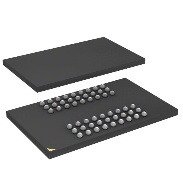
| Device Package | 54-TFBGA (8x13) | Memory Format | DRAM | Technology | SDRAM | ||
|---|---|---|---|---|---|---|---|
| Memory Size | 256 Mbit | Access Time | 5.4 ns | Grade | Industrial | ||
| Clock Frequency | 166 MHz | Voltage | 3V ~ 3.6V | Memory Type | Volatile | ||
| Operating Temperature | -40°C ~ 85°C (TA) | Write Cycle Time Word Page | N/A | Packaging | 54-TFBGA | ||
| Mounting Method | Volatile | Memory Interface | Parallel | Memory Organization | 16M x 16 | ||
| Moisture Sensitivity Level | 3 (168 Hours) | RoHS Compliance | ROHS3 Compliant | REACH Compliance | REACH Unaffected | ||
| Qualification | N/A | ECCN | EAR99 | HTS Code | 8542.32.0002 |
Overview of IS45S16160D-6BLA1-TR – 256Mbit SDRAM, 54‑TFBGA
The IS45S16160D-6BLA1-TR is a 256‑Mbit synchronous DRAM organized as 16M × 16 with a parallel memory interface. It uses a pipeline architecture and fully synchronous operation referenced to a positive clock edge to support high‑speed, deterministic data transfers.
This device targets designs requiring standard SDRAM functionality with programmable burst control, selectable CAS latency, and on‑chip refresh features, supplied in a compact 54‑ball TFBGA package and specified for operation from -40°C to +85°C.
Key Features
- Memory Type & Capacity 256 Mbit SDRAM organized as 16M × 16 providing parallel DRAM storage.
- High‑speed Synchronous Interface Fully synchronous SDRAM with clock frequency up to 166 MHz (CL=3) and LVTTL I/O signaling.
- Low Latency Performance Access time from clock as low as 5.4 ns (CAS latency = 3) with programmable CAS latency options of 2 or 3 clocks.
- Flexible Burst Control Programmable burst lengths (1, 2, 4, 8, full page) and selectable burst sequence (sequential or interleave) for optimized data transfer patterns.
- Refresh and Power Management Supports Auto Refresh and Self Refresh; refresh options include 8K cycles every 16 ms or 64 ms depending on grade.
- Internal Bank Architecture Internal bank structure to hide row access and precharge delays, improving effective throughput for random access patterns.
- Power Supply Single power supply operation across a nominal 3.0 V to 3.6 V range (datasheet lists 3.3 V ±0.3 V).
- Package 54‑TFBGA (54‑ball BGA, 8 × 13) compact package suitable for surface‑mount applications.
- Operating Temperature Specified ambient range of -40°C to +85°C (TA).
Typical Applications
- High‑speed memory subsystems — Provides synchronous parallel DRAM storage for systems requiring predictable, clocked access and burst transfers.
- Data buffering — Suitable for buffering and temporary storage where programmable burst length and low access time improve throughput.
- Embedded system memory — Can serve as the main external SDRAM in embedded designs that operate at 3.0–3.6 V and require a compact BGA footprint.
Unique Advantages
- Clocked, deterministic operation: Fully synchronous design referenced to the rising clock edge enables predictable timing for system designers.
- Flexible timing and bursts: Programmable CAS latency, burst length and sequence allow tuning for varied access patterns and system requirements.
- On‑chip refresh options: Auto Refresh and Self Refresh modes with selectable refresh intervals reduce external refresh management complexity.
- Compact board footprint: 54‑ball TFBGA (8×13) package minimizes PCB area for space‑constrained designs.
- Robust temperature range: Specified operation from -40°C to +85°C supports commercial and industrial ambient conditions.
Why Choose IC DRAM 256MBIT PAR 54TFBGA?
The IS45S16160D-6BLA1-TR delivers a straightforward, standards‑based 256‑Mbit SDRAM solution combining synchronous pipeline architecture, programmable burst behavior, and selectable CAS latency to meet a range of clocked memory requirements. Its 16M × 16 organization and parallel LVTTL interface make it suitable where deterministic timing and burst transfers are required.
With on‑chip refresh features, a single 3.0–3.6 V supply range, and a compact 54‑TFBGA package, this device is appropriate for designs needing reliable SDRAM performance in a small footprint and an ambient operating range down to -40°C.
Request a quote or submit a parts inquiry to receive pricing and availability information for IS45S16160D-6BLA1-TR.