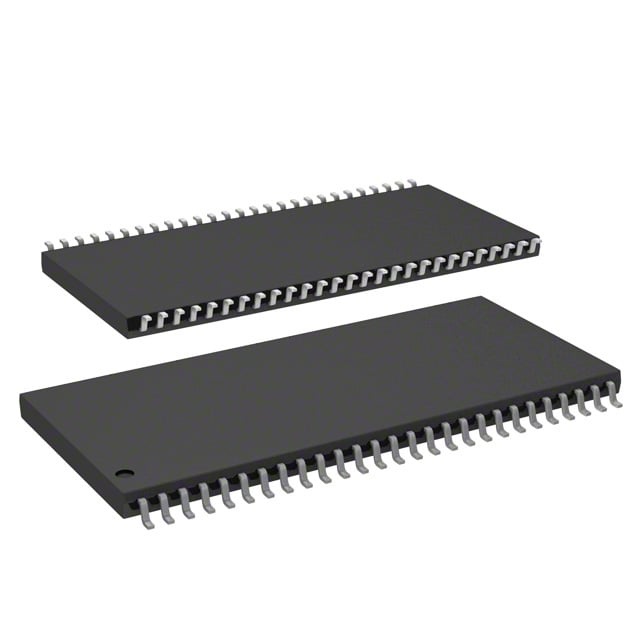
IS45S16160G-7TLA1
| Part Description |
IC DRAM 256MBIT PAR 54TSOP II |
|---|---|
| Quantity | 186 Available (as of June 14, 2026) |

| Product Category | Memory |
|---|---|
| Manufacturer | Integrated Silicon Solution Inc |
| Manufacturing Status | Obsolete |
| Manufacturer Standard Lead Time | Contact Us |
| Datasheet |
Specifications & Environmental
| Device Package | 54-TSOP II | Memory Format | DRAM | Technology | SDRAM | ||
|---|---|---|---|---|---|---|---|
| Memory Size | 256 Mbit | Access Time | 5.4 ns | Grade | Industrial | ||
| Clock Frequency | 143 MHz | Voltage | 3V ~ 3.6V | Memory Type | Volatile | ||
| Operating Temperature | -40°C ~ 85°C (TA) | Write Cycle Time Word Page | N/A | Packaging | 54-TSOP (0.400", 10.16mm Width) | ||
| Mounting Method | Volatile | Memory Interface | Parallel | Memory Organization | 16M x 16 | ||
| Moisture Sensitivity Level | 3 (168 Hours) | RoHS Compliance | ROHS3 Compliant | REACH Compliance | REACH Unaffected | ||
| Qualification | N/A | ECCN | EAR99 | HTS Code | 8542.32.0028 |
Overview of IS45S16160G-7TLA1 – IC DRAM 256Mbit Parallel 54‑TSOP II
The IS45S16160G-7TLA1 is a 256 Mbit synchronous DRAM organized as 16M × 16 with internal banks and a parallel memory interface. It implements a fully synchronous pipeline architecture with programmable burst modes and CAS latency options to support high-speed, predictable data transfers for memory buffer and working storage applications.
Designed for systems requiring a single-supply 3.3 V memory solution, this device delivers operation at up to 143 MHz with a 5.4 ns access time and supports industry-standard refresh and self-refresh functions to maintain data integrity across a wide operating temperature range.
Key Features
- Memory Core Organized as 16M × 16 (256 Mbit) with internal bank architecture (4 banks) to hide row access and precharge latency.
- Performance Clock frequency up to 143 MHz with an access time of 5.4 ns (CAS latency selectable), supporting burst read/write operations and programmable burst lengths (1, 2, 4, 8, full page).
- Synchronous Interface Fully synchronous SDRAM with LVTTL-compatible signaling and all signals referenced to the positive clock edge for deterministic timing.
- Refresh and Power Management Auto Refresh and Self Refresh supported; 8K refresh cycles every 32 ms or 64 ms depending on grade options to maintain data retention.
- Programmability Programmable CAS latency (2 or 3 clocks) and programmable burst sequence (sequential or interleave) to match system timing and access patterns.
- Power Single power supply operation at 3.0 V to 3.6 V (typical 3.3 V ±0.3 V).
- Package and Temperature Available in a 54-pin TSOP‑II package (0.400", 10.16 mm width) and specified for an operating temperature range of −40 °C to +85 °C (TA).
Typical Applications
- High‑speed buffer memory Systems that require a 256 Mbit parallel SDRAM for temporary data buffering and rapid burst transfers, leveraging the 143 MHz clock and programmable burst modes.
- Frame and line memory Video and imaging subsystems that need predictable, synchronous read/write timing and selectable CAS latency for streaming data.
- Embedded system working memory Microprocessor and FPGA-based designs that require a single-supply 3.3 V SDRAM with self-refresh and auto-refresh support across a −40 °C to +85 °C operating range.
Unique Advantages
- Deterministic synchronous operation: Fully synchronous design with LVTTL interface ensures signals are referenced to the clock edge for predictable timing.
- Flexible access patterns: Programmable burst length and sequence plus CAS latency options let designers optimize throughput and latency for varied access patterns.
- Integrated bank architecture: Internal bank structure hides row access/precharge delays to improve effective bandwidth for burst transfers.
- Robust refresh options: Auto Refresh and Self Refresh support with 8K cycles per refresh interval provides reliable data retention across grades.
- Industry-standard package: 54‑pin TSOP‑II (10.16 mm width) provides a compact footprint for board-level integration in space-constrained designs.
Why Choose IS45S16160G-7TLA1?
The IS45S16160G-7TLA1 delivers a compact, single‑supply 256 Mbit SDRAM solution with configurable latency and burst behavior, making it suitable for designs that require predictable, high‑speed parallel memory. Its synchronous pipeline architecture, internal banking, and refresh capabilities provide designers with the controls needed to tune performance and reliability for a wide range of embedded and system‑level memory functions.
This device is appropriate for engineers building systems that need a 3.3 V parallel SDRAM with defined timing (143 MHz, 5.4 ns access) and a rugged operating temperature range; it offers straightforward integration into memory subsystems where deterministic synchronous behavior and selectable burst modes are required.
Request a quote or submit an inquiry for pricing and lead-time information to evaluate the IS45S16160G-7TLA1 for your design.