IS45S16160G-7CTLA1-TR
| Part Description |
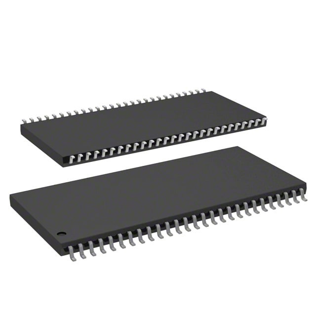
IC DRAM 256MBIT PAR 54TSOP II |
|---|---|
| Quantity | 1,253 Available (as of June 15, 2026) |

| Product Category | Memory |
|---|---|
| Manufacturer | Integrated Silicon Solution Inc |
| Manufacturing Status | Obsolete |
| Manufacturer Standard Lead Time | Contact Us |
| Datasheet |
Specifications & Environmental
| Device Package | 54-TSOP II | Memory Format | DRAM | Technology | SDRAM | ||
|---|---|---|---|---|---|---|---|
| Memory Size | 256 Mbit | Access Time | 5.4 ns | Grade | Industrial | ||
| Clock Frequency | 143 MHz | Voltage | 3V ~ 3.6V | Memory Type | Volatile | ||
| Operating Temperature | -40°C ~ 85°C (TA) | Write Cycle Time Word Page | N/A | Packaging | 54-TSOP (0.400", 10.16mm Width) | ||
| Mounting Method | Volatile | Memory Interface | Parallel | Memory Organization | 16M x 16 | ||
| Moisture Sensitivity Level | 3 (168 Hours) | RoHS Compliance | ROHS Compliant | REACH Compliance | REACH Unaffected | ||
| Qualification | N/A | ECCN | EAR99 | HTS Code | 8542.32.0028 |
Overview of IS45S16160G-7CTLA1-TR – IC DRAM 256MBIT PAR 54TSOP II
The IS45S16160G-7CTLA1-TR is a 256 Mbit synchronous DRAM (SDRAM) organized as 16M × 16 with a parallel interface. It implements a pipelined, fully synchronous architecture with internal banks and standard SDRAM control for high-speed data transfer in board-level memory subsystems.
Targeted for embedded and industrial applications, this device offers a 143 MHz clock option with low access latency and a compact 54-pin TSOP-II package, enabling performance-driven memory expansion where a 3.3 V supply and industrial temperature range are required.
Key Features
- Memory Core 256 Mbit SDRAM, organized as 16M × 16 with 4 internal banks for concurrent row management and improved throughput.
- Synchronous, Pipelined Operation Fully synchronous design with all signals referenced to the rising clock edge; pipeline architecture for high-speed transfers at the specified clock rate.
- Performance Rated for a 143 MHz clock (–7 speed grade) with an access time from clock of 5.4 ns and programmable CAS latency (2 or 3 clocks).
- Burst and Sequencing Programmable burst lengths (1, 2, 4, 8, full page) and selectable sequential or interleaved burst sequences for flexible burst read/write behavior.
- Refresh and Retention Auto-refresh and self-refresh support with 8K refresh cycles; refresh interval varies by grade (32 ms or 64 ms as specified for grade).
- Interface and Supply LVTTL-compatible interface and single power-supply operation at 3.0 V to 3.6 V (3.3 V ±0.3 V), simplifying integration with standard 3.3 V systems.
- Package and Temperature 54-pin TSOP-II package (0.400" / 10.16 mm width) and an operating ambient temperature range of −40 °C to +85 °C (TA) for industrial use.
Typical Applications
- Embedded Systems External system memory for microprocessor- or FPGA-based designs that require synchronous DRAM with a parallel interface and mid-range clock performance.
- Industrial Control Memory expansion in industrial controllers and instrumentation where the −40 °C to +85 °C operating range and 3.3 V supply are required.
- Buffering and Caching Frame buffers, packet buffers, or cache/burst buffers that benefit from the device’s burst modes, internal bank architecture, and low access latency.
- Networking and Communications Board-level memory for networking equipment that needs synchronous, low-latency data staging and high-throughput transfers.
Unique Advantages
- Deterministic Synchronous Timing Fully synchronous operation referenced to clock edges enables predictable timing for system-level memory control and timing closure.
- Flexible Burst Control Programmable burst lengths and sequences allow designers to optimize throughput and bus utilization for diverse data patterns.
- Industry-Standard Voltage and Interface LVTTL signaling and a 3.0 V–3.6 V supply align with common 3.3 V system rails, easing integration into existing designs.
- Industrial Temperature Support Rated for −40 °C to +85 °C ambient operation, suitable for many industrial-grade applications.
- Compact TSOP-II Footprint 54-pin TSOP-II (10.16 mm width) package supports compact board layouts while providing the full 16-bit data width.
- Built-in Refresh Management Auto-refresh and self-refresh features simplify system-level DRAM maintenance and support low-power retention modes.
Why Choose IS45S16160G-7CTLA1-TR?
The IS45S16160G-7CTLA1-TR delivers a balance of synchronous SDRAM performance, flexible burst operation, and industrial temperature capability in a compact 54-pin TSOP-II package. Its 16M × 16 organization, internal bank structure, and programmable timing features make it suitable for designs that require predictable, board-level DRAM performance on a 3.3 V platform.
This device is appropriate for engineers specifying external SDRAM for embedded controllers, industrial systems, networking equipment, and buffering applications that need a 256 Mbit capacity with mid-range clock and low access latency.
Request a quote or submit an inquiry for pricing and availability of IS45S16160G-7CTLA1-TR to receive lead-time and volume pricing information.