IS45S16160G-7CTLA2
| Part Description |
IC DRAM 256MBIT PAR 54TSOP II |
|---|---|
| Quantity | 458 Available (as of June 15, 2026) |
| Product Category | DRAM Memory |
|---|---|
| Manufacturer | Integrated Silicon Solution Inc |
| Manufacturing Status | Obsolete |
| Manufacturer Standard Lead Time | Contact Us |
| Datasheet |
Specifications & Environmental
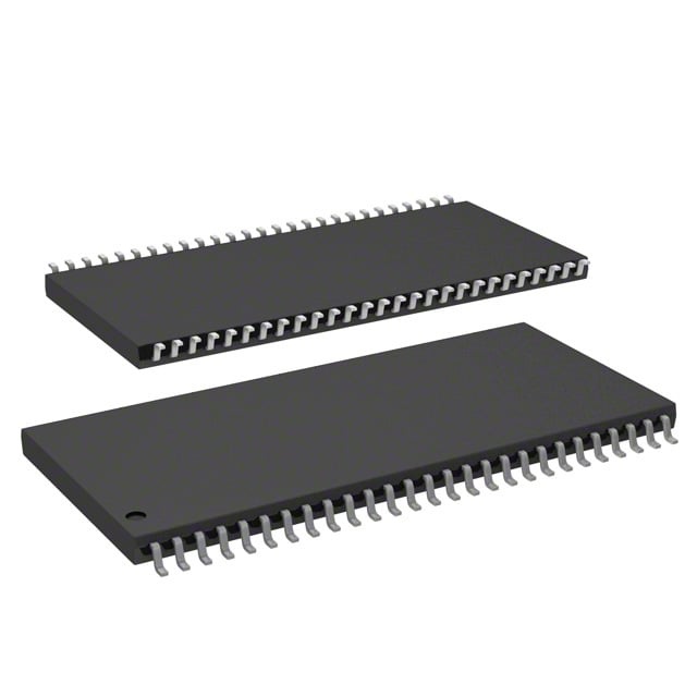
| Device Package | 54-TSOP II | Memory Format | DRAM | Technology | SDRAM | ||
|---|---|---|---|---|---|---|---|
| Memory Size | 256 Mbit | Access Time | 5.4 ns | Grade | Automotive | ||
| Clock Frequency | 143 MHz | Voltage | 3V ~ 3.6V | Memory Type | Volatile | ||
| Operating Temperature | -40°C ~ 105°C (TA) | Write Cycle Time Word Page | N/A | Packaging | 54-TSOP (0.400", 10.16mm Width) | ||
| Mounting Method | Volatile | Memory Interface | Parallel | Memory Organization | 16M x 16 | ||
| Moisture Sensitivity Level | 3 (168 Hours) | RoHS Compliance | ROHS3 Compliant | REACH Compliance | REACH Unaffected | ||
| Qualification | N/A | ECCN | EAR99 | HTS Code | 8542.32.0028 |
Overview of IS45S16160G-7CTLA2 – 256 Mbit SDRAM, 54‑pin TSOP II
The IS45S16160G-7CTLA2 is a 256 Mbit synchronous DRAM organized as 16M × 16 with a parallel memory interface and a 54‑pin TSOP II package. It implements a fully synchronous pipeline architecture with internal bank management to support high‑speed data transfer and predictable timing behavior.
Targeted for designs requiring parallel SDRAM memory with programmable burst operation and selectable CAS latency, this device delivers deterministic access timing across a wide operating temperature range and a 3.0 V–3.6 V supply window.
Key Features
- Core / Architecture Fully synchronous SDRAM with internal bank architecture for row access/precharge hiding and predictable, clock‑referenced operation.
- Memory Organization 256 Mbit capacity arranged as 16M × 16 with four internal banks.
- Performance -7 speed grade supports a clock frequency up to 143 MHz and access times of 5.4 ns (CAS latency options apply).
- Programmable Burst and CAS Programmable burst lengths (1, 2, 4, 8, full page) and burst sequences (sequential/interleave), with selectable CAS latency of 2 or 3 clocks.
- Refresh and Low‑Power Modes Auto Refresh (CBR) and Self Refresh support; 8K refresh cycles per specified interval per device grade.
- Interface and I/O LVTTL compatible interface with synchronous, edge‑referenced signaling and support for random column address every clock cycle.
- Power Single power supply operation across 3.0 V to 3.6 V.
- Package and Temperature 54‑pin TSOP II (0.400", 10.16 mm width) package; specified operating temperature range from −40°C to +105°C (TA).
Typical Applications
- Parallel memory subsystems Acts as system memory or buffer where a parallel SDRAM interface and 16‑bit data path are required.
- Embedded and industrial equipment Suitable for designs that need synchronous DRAM with wide operating temperature support and programmable timing.
- High‑throughput buffering Used for burst read/write buffering in systems that leverage programmable burst lengths and internal bank management.
Unique Advantages
- Deterministic synchronous timing All signals referenced to the positive clock edge for predictable timing and easy integration into clocked systems.
- Flexible burst and latency control Programmable burst lengths, burst sequences, and CAS latency options enable tuning for different access patterns and system timing.
- High‑speed operation -7 speed grade supports up to 143 MHz operation with 5.4 ns access times for responsive data transfers.
- Robust refresh and power modes Auto and self refresh support with defined refresh cycles to maintain data integrity while managing power.
- Compact package 54‑pin TSOP II footprint provides a space‑efficient mounting option for board designs requiring parallel SDRAM.
- Wide supply tolerance Operates across a 3.0 V–3.6 V supply range to accommodate common 3.3 V system rails.
Why Choose IC DRAM 256MBIT PAR 54TSOP II?
The IS45S16160G-7CTLA2 positions itself as a solid choice for systems requiring a 16‑bit parallel SDRAM with programmable burst behavior, selectable CAS latency, and predictable synchronous timing. Its combination of 256 Mbit capacity, internal bank architecture, and up to 143 MHz clocking supports applications that need responsive burst reads/writes and deterministic memory access.
This device is well suited for engineers specifying parallel SDRAM in embedded or industrial designs that demand a compact TSOP II package, defined refresh behavior, and a 3.0 V–3.6 V power envelope. The feature set enables straightforward integration into clocked memory subsystems while allowing timing and burst configuration to match application requirements.
Request a quote or submit an inquiry to receive pricing and availability information for the IS45S16160G-7CTLA2.