IS45S16160G-7TLA2
| Part Description |
IC DRAM 256MBIT PAR 54TSOP II |
|---|---|
| Quantity | 652 Available (as of June 14, 2026) |

| Product Category | Memory |
|---|---|
| Manufacturer | Integrated Silicon Solution Inc |
| Manufacturing Status | Obsolete |
| Manufacturer Standard Lead Time | Contact Us |
| Datasheet |
Specifications & Environmental
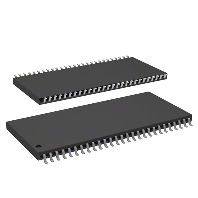
| Device Package | 54-TSOP II | Memory Format | DRAM | Technology | SDRAM | ||
|---|---|---|---|---|---|---|---|
| Memory Size | 256 Mbit | Access Time | 5.4 ns | Grade | Automotive | ||
| Clock Frequency | 143 MHz | Voltage | 3V ~ 3.6V | Memory Type | Volatile | ||
| Operating Temperature | -40°C ~ 105°C (TA) | Write Cycle Time Word Page | N/A | Packaging | 54-TSOP (0.400", 10.16mm Width) | ||
| Mounting Method | Volatile | Memory Interface | Parallel | Memory Organization | 16M x 16 | ||
| Moisture Sensitivity Level | 3 (168 Hours) | RoHS Compliance | ROHS3 Compliant | REACH Compliance | REACH Unaffected | ||
| Qualification | N/A | ECCN | EAR99 | HTS Code | 8542.32.0028 |
Overview of IS45S16160G-7TLA2 – IC DRAM 256MBIT PAR 54TSOP II
The IS45S16160G-7TLA2 is a 256 Mbit synchronous DRAM (SDRAM) device organized as 16M × 16 with a parallel memory interface. It uses a pipeline architecture and fully synchronous signaling referenced to a positive clock edge for high-speed data transfer in systems that require deterministic SDRAM behavior.
Designed for systems operating from a single 3.3 V supply (3.0 V to 3.6 V), the device offers programmable burst modes, selectable CAS latency, internal bank architecture for hidden row access/precharge, and support for Auto Refresh and Self Refresh modes. The device is available in a 54-pin TSOP II package with a 10.16 mm width.
Key Features
- Memory Core 256 Mbit SDRAM organized as 16M × 16 with internal bank architecture to improve effective access performance.
- Performance Clock frequency support up to 143 MHz for the -7 speed grade; access time from clock as low as 5.4 ns (CL = 3).
- Programmable Burst & Latency Programmable burst lengths (1, 2, 4, 8, full page) and selectable burst sequence (Sequential/Interleave); CAS latency programmable between 2 and 3 clocks.
- Refresh and Power Management Supports Auto Refresh (CBR) and Self Refresh; 8K refresh cycles per refresh period as specified for commercial and grade options.
- Interface LVTTL-compatible signals with a parallel memory interface for systems using standard SDRAM control timing.
- Supply Voltage Single power supply operation from 3.0 V to 3.6 V (nominal 3.3 V ±0.3 V).
- Package & Mounting 54-pin TSOP II package (0.400" / 10.16 mm width) for surface-mount applications.
- Operating Temperature Rated for operation from −40°C to +105°C (TA) depending on device grade.
Typical Applications
- Synchronous system memory Use as main SDRAM in systems that require pipeline synchronous DRAM with programmable burst and latency options.
- High-speed data buffering Buffering and temporary storage where deterministic, clock-referenced transfers and low access times (5.4 ns from clock) are required.
- Parallel-interface designs Integration into legacy or contemporary designs using a parallel LVTTL SDRAM interface and standard SDRAM control signals.
- Wide-temperature deployments Applications requiring extended ambient temperature capability (specified down to −40°C and up to +105°C TA for applicable grades).
Unique Advantages
- Flexible performance scaling: Programmable burst lengths and CAS latencies let designers balance throughput and latency for target workloads.
- Predictable low-latency access: Access times from clock as low as 5.4 ns (CL = 3) at the -7 speed grade provide predictable read timing for real-time data paths.
- Single-supply simplicity: Operates from a single 3.0 V–3.6 V supply, simplifying power-supply design and integration.
- Internal bank architecture: Built-in bank management hides row access/precharge latency to improve effective throughput on burst operations.
- Standard package footprint: 54-pin TSOP II (10.16 mm width) supports common board-level mounting and form-factor constraints.
- Comprehensive refresh modes: Auto Refresh and Self Refresh support with specified refresh cycles for continuous data integrity management.
Why Choose IS45S16160G-7TLA2?
The IS45S16160G-7TLA2 delivers a well-specified synchronous DRAM solution for designs that need 256 Mbit of parallel SDRAM capacity with programmable burst behavior and selectable CAS latency. Its pipeline architecture, internal bank management, and low access times enable predictable high-speed data transfers in systems that rely on clocked memory operations.
This device is appropriate for engineers and procurement teams specifying SDRAM for projects that require a 3.3 V single-supply memory, a 54-pin TSOP II package, and operation across a wide ambient temperature range. The combination of programmable performance options, standard interface levels, and refresh management supports long-term design stability and integration into established SDRAM architectures.
If you would like pricing, lead-time information, or a formal quote for the IS45S16160G-7TLA2, please submit a request or inquiry and our team will respond with details.