IS45S16160G-7TLA2-TR
| Part Description |
IC DRAM 256MBIT PAR 54TSOP II |
|---|---|
| Quantity | 35 Available (as of June 18, 2026) |

| Product Category | DRAM Memory |
|---|---|
| Manufacturer | Integrated Silicon Solution Inc |
| Manufacturing Status | Obsolete |
| Manufacturer Standard Lead Time | Contact Us |
| Datasheet |
Specifications & Environmental
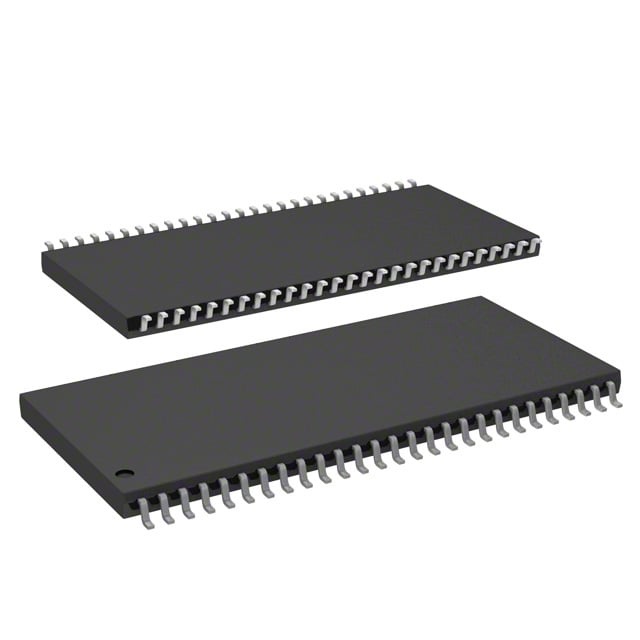
| Device Package | 54-TSOP II | Memory Format | DRAM | Technology | SDRAM | ||
|---|---|---|---|---|---|---|---|
| Memory Size | 256 Mbit | Access Time | 5.4 ns | Grade | Automotive | ||
| Clock Frequency | 143 MHz | Voltage | 3V ~ 3.6V | Memory Type | Volatile | ||
| Operating Temperature | -40°C ~ 105°C (TA) | Write Cycle Time Word Page | N/A | Packaging | 54-TSOP (0.400", 10.16mm Width) | ||
| Mounting Method | Volatile | Memory Interface | Parallel | Memory Organization | 16M x 16 | ||
| Moisture Sensitivity Level | 3 (168 Hours) | RoHS Compliance | ROHS3 Compliant | REACH Compliance | REACH Unaffected | ||
| Qualification | N/A | ECCN | EAR99 | HTS Code | 8542.32.0028 |
Overview of IS45S16160G-7TLA2-TR – IC DRAM 256 Mbit Parallel SDRAM, 54‑TSOP II
The IS45S16160G-7TLA2-TR is a 256 Mbit synchronous DRAM organized as 16M × 16 with a parallel memory interface. It uses a pipelined, fully synchronous architecture with internal bank management and LVTTL signaling to support high-speed data transfer and burst operations.
This device is targeted at designs that require a compact 54‑pin TSOP‑II memory package, programmable burst sequencing and latency, and operation from a 3.0 V to 3.6 V supply across an extended temperature range.
Key Features
- Core / Architecture Fully synchronous SDRAM; all signals referenced to the rising edge of the clock and built with internal banks for row access/precharge hiding.
- Memory Organization 256 Mbit capacity arranged as 16M × 16 with four internal banks.
- Performance Clock frequency up to 143 MHz (‑7 speed grade) with access time from clock as low as 5.4 ns for listed latency configurations.
- Interface Parallel memory interface with LVTTL signaling and programmable burst length (1, 2, 4, 8, full page) and burst sequence (sequential/interleave).
- Timing & Programmability Programmable CAS latency (2 or 3 clocks), random column address every clock cycle, and support for burst read/write and burst read/single write operations with burst termination commands.
- Refresh & Power Auto Refresh (CBR) and Self Refresh support; refresh intervals include 8K cycles every 32 ms or 64 ms depending on device grade. Single power supply: 3.3 V ± 0.3 V (documented supply range 3.0 V–3.6 V).
- Package & Temperature 54‑pin TSOP‑II package (0.400", 10.16 mm width) with operating temperature documented to −40 °C to +105 °C (TA) for the specified device variant.
Typical Applications
- High‑speed data buffering Use where pipelined, synchronous memory is required for rapid data transfer and temporary storage.
- System memory expansion Parallel SDRAM option for designs needing a 256 Mbit organized memory device with programmable burst behavior and bank management.
- Industrial and extended‑temperature electronics Suitable for systems that require operation to −40 °C and up to +105 °C (TA) with a compact TSOP‑II footprint.
Unique Advantages
- 256 Mbit density in a compact package: Offers 16M × 16 organization in a 54‑pin TSOP‑II to minimize board area for mid‑density memory requirements.
- Programmable burst and latency: Burst length and sequence plus CAS latency options provide flexibility to match memory timing to system requirements.
- Pipelined synchronous operation: Fully synchronous interface with internal bank management enables predictable timing and efficient high‑speed transfers.
- Extended temperature support: Specified operation down to −40 °C and up to +105 °C (TA) for designs with wider thermal requirements.
- Standard 3.3 V supply compatibility: Operates from 3.0 V to 3.6 V (documented as 3.3 V ±0.3 V), aligning with common system power rails.
Why Choose IC DRAM 256MBIT PAR 54TSOP II?
The IS45S16160G-7TLA2-TR is positioned for designs that need a mid‑density, fully synchronous DRAM with programmable burst behavior, predictable timing, and compact TSOP‑II packaging. Its 16M × 16 organization, support for programmable CAS latency and burst modes, and pipelined bank architecture deliver the configurability and throughput required for high‑speed buffering and system memory roles.
This device is suited to engineers and procurement teams specifying a 256 Mbit parallel SDRAM that must operate from a 3.0 V–3.6 V supply and meet extended ambient temperature requirements while retaining flexible timing and refresh options.
Request a quote or submit a pricing inquiry to evaluate the IS45S16160G-7TLA2-TR for your next design.