IS45S16160G-7CTLA2-TR
| Part Description |
IC DRAM 256MBIT PAR 54TSOP II |
|---|---|
| Quantity | 18 Available (as of June 15, 2026) |

| Product Category | Memory |
|---|---|
| Manufacturer | Integrated Silicon Solution Inc |
| Manufacturing Status | Obsolete |
| Manufacturer Standard Lead Time | Contact Us |
| Datasheet |
Specifications & Environmental
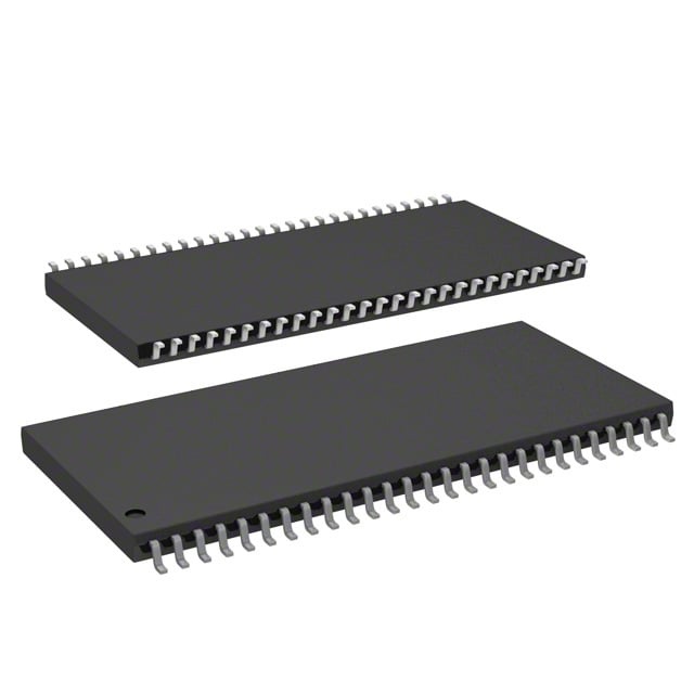
| Device Package | 54-TSOP II | Memory Format | DRAM | Technology | SDRAM | ||
|---|---|---|---|---|---|---|---|
| Memory Size | 256 Mbit | Access Time | 5.4 ns | Grade | Automotive | ||
| Clock Frequency | 143 MHz | Voltage | 3V ~ 3.6V | Memory Type | Volatile | ||
| Operating Temperature | -40°C ~ 105°C (TA) | Write Cycle Time Word Page | N/A | Packaging | 54-TSOP (0.400", 10.16mm Width) | ||
| Mounting Method | Volatile | Memory Interface | Parallel | Memory Organization | 16M x 16 | ||
| Moisture Sensitivity Level | 3 (168 Hours) | RoHS Compliance | ROHS Compliant | REACH Compliance | REACH Unaffected | ||
| Qualification | N/A | ECCN | EAR99 | HTS Code | 8542.32.0028 |
Overview of IS45S16160G-7CTLA2-TR – 256Mbit SDRAM 54-TSOP II
The IS45S16160G-7CTLA2-TR from Integrated Silicon Solution Inc. (ISSI) is a 256Mbit synchronous DRAM organized as 16M × 16 with internal bank architecture and pipeline operation. It provides a fully synchronous, parallel SDRAM interface designed for systems that require predictable, clock-referenced memory access and programmable burst operation.
Built for designs that require high-density parallel SDRAM in a compact 54-pin TSOP-II package, the device emphasizes synchronous timing control, programmable burst modes and refresh management for reliable data storage in volatile memory applications.
Key Features
- Memory Architecture — 256 Mbit capacity organized as 16M × 16 with internal banks to hide row access/precharge and support random column access every clock cycle.
- Synchronous SDRAM Core — Fully synchronous operation with all inputs/outputs referenced to the rising edge of the clock; pipeline architecture for high-speed data transfer.
- Speed and Timing — -7 speed grade supports a clock frequency up to 143 MHz with access time from clock of 5.4 ns and programmable CAS latency (2 or 3 clocks).
- Burst Control — Programmable burst length (1, 2, 4, 8, full page) and selectable burst sequence (sequential or interleave); supports burst read/write and burst read/single write operations with burst termination commands.
- Refresh and Self-Refresh — Auto Refresh (CBR) and Self Refresh supported; 8K refresh cycles with selectable refresh period options (32 ms for A2 grade or 64 ms for commercial/industrial and A1 grade) as specified.
- Interface and I/O — Parallel memory interface with LVTTL-compatible signaling for command and control.
- Power — Single power supply, 3.3 V nominal (3.0 V to 3.6 V supply range).
- Package and Mounting — 54-pin TSOP-II (0.400", 10.16 mm width) package suited for surface-mount assembly.
- Operating Temperature — Rated for operation from -40°C to +105°C (TA) per product specification.
Typical Applications
- Embedded Memory Modules — Provides high-density parallel SDRAM storage for embedded systems requiring synchronous, burst-capable memory.
- Board-Level DRAM — Fits designs that need 256 Mbit SDRAM in a compact 54-pin TSOP-II footprint for space-constrained PCBs.
- Systems Requiring Flexible Burst Access — Useful where programmable burst length and sequence (sequential/interleave) are needed to tune throughput and latency.
Unique Advantages
- High-density 256 Mbit capacity: Enables larger on-board memory without increasing package pin count, simplifying memory scaling.
- Programmable performance parameters: CAS latency, burst length and burst sequence settings allow designers to match memory timing to system requirements.
- Robust refresh options: Auto and self-refresh with selectable refresh intervals accommodate different operational and power scenarios.
- Compact TSOP-II package: 54-pin TSOP-II (10.16 mm width) provides a compact SMD solution for board designs constrained by area or routing.
- Wide operating temperature range: -40°C to +105°C rating supports deployment in temperature-challenging environments.
- Standard 3.3 V supply: Nominal single-supply operation (3.0–3.6 V) aligns with common system power rails for simplified integration.
Why Choose IS45S16160G-7CTLA2-TR?
The IS45S16160G-7CTLA2-TR is positioned for designs that require a high-density, fully synchronous parallel SDRAM with flexible burst control and robust refresh management. Its 16M × 16 organization, programmable timing (CAS latency 2/3) and 143 MHz clock grade (-7) offer a clear balance of capacity, timing flexibility and predictable, clock-referenced access.
This device is suitable for engineers specifying compact, board-level DRAM in a 54-pin TSOP-II package who need controllable burst behavior, LVTTL command signaling and an extended operating temperature range. The combination of density, synchronous pipeline operation and selectable refresh modes supports scalable implementations where verified timing and reliable volatile storage are required.
Request a quote or submit an inquiry to receive pricing and availability information for the IS45S16160G-7CTLA2-TR.