IS45S16160G-7BLA2-TR
| Part Description |
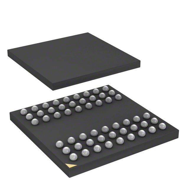
IC DRAM 256MBIT PAR 54TFBGA |
|---|---|
| Quantity | 392 Available (as of June 15, 2026) |

| Product Category | DRAM Memory |
|---|---|
| Manufacturer | Integrated Silicon Solution Inc |
| Manufacturing Status | Obsolete |
| Manufacturer Standard Lead Time | Contact Us |
| Datasheet |
Specifications & Environmental
| Device Package | 54-TFBGA (8x8) | Memory Format | DRAM | Technology | SDRAM | ||
|---|---|---|---|---|---|---|---|
| Memory Size | 256 Mbit | Access Time | 5.4 ns | Grade | Automotive | ||
| Clock Frequency | 143 MHz | Voltage | 3V ~ 3.6V | Memory Type | Volatile | ||
| Operating Temperature | -40°C ~ 105°C (TA) | Write Cycle Time Word Page | N/A | Packaging | 54-TFBGA | ||
| Mounting Method | Volatile | Memory Interface | Parallel | Memory Organization | 16M x 16 | ||
| Moisture Sensitivity Level | 3 (168 Hours) | RoHS Compliance | ROHS3 Compliant | REACH Compliance | REACH Unaffected | ||
| Qualification | N/A | ECCN | EAR99 | HTS Code | 8542.32.0028 |
Overview of IS45S16160G-7BLA2-TR – 256Mbit SDRAM, 54‑TFBGA
The IS45S16160G-7BLA2-TR is a 256 Mbit synchronous DRAM device organized as 16M × 16 bits with internal bank architecture and a parallel memory interface. It implements a fully synchronous, pipelined architecture with all signals referenced to the rising clock edge and is offered in a 54‑ball TFBGA (8×8) package.
Designed for systems that require a 3.3 V class parallel SDRAM with programmable burst operation and selectable CAS latency, this device supports timing grade −7 (143 MHz clock, 5.4 ns access time) and offers features for sustained data transfers and refresh management across extended temperature ranges.
Key Features
- Memory Core — 256 Mbit SDRAM organized as 16M × 16 with 4 internal banks for row access/precharge hiding and improved pipeline throughput.
- Performance — Timing grade −7 supports a clock frequency of 143 MHz with an access time from clock of 5.4 ns; programmable CAS latency of 2 or 3 clocks.
- Burst and Sequencing — Programmable burst lengths (1, 2, 4, 8, full page) and selectable burst sequence (Sequential/Interleave) with burst read/write and burst read/single write capability; burst termination via stop or precharge command.
- Refresh and Self-Refresh — Auto Refresh (CBR) and Self Refresh supported; refresh options include 8K cycles per 32 ms (A2 grade) or 64 ms (commercial/industrial/A1 grade).
- Interface and Logic Levels — Fully synchronous interface with LVTTL signaling referenced to the positive clock edge; random column address every clock cycle.
- Power — Single power supply operation at 3.3 V ±0.3 V (3.0 V to 3.6 V supply range).
- Package and Temperature — 54‑TFBGA (8×8) ball array package; operating temperature range shown as −40 °C to +105 °C (TA) for the specified device grade.
Typical Applications
- High-throughput buffering — Pipeline architecture and burst modes for applications requiring sustained synchronous data transfers and buffering.
- Parallel memory subsystems — 16‑bit wide organization and parallel interface for systems needing a 256 Mbit SDRAM memory bank.
- Extended temperature environments — Device options and specified operating range down to −40 °C and up to +105 °C for designs requiring broader TA coverage.
Unique Advantages
- Pipelined synchronous design: All I/O referenced to the rising clock edge and internal banking enable predictable timing and effective throughput for synchronous systems.
- Flexible burst control: Programmable burst lengths and sequence modes simplify data-transfer scheduling and optimize bus utilization.
- Selectable CAS latency: CAS latency options (2 or 3 clocks) allow tuning for system timing requirements and performance trade-offs.
- Comprehensive refresh modes: Auto and self‑refresh support with configurable refresh intervals (8K cycles/32 ms or 64 ms) help maintain data integrity across operating conditions.
- Standard 3.3 V supply: Single 3.3 V ±0.3 V power rail simplifies system power design and integration.
- Compact BGA package: 54‑ball TFBGA (8×8) provides a small-footprint assembly option for space-constrained PCBs.
Why Choose IS45S16160G-7BLA2-TR?
The IS45S16160G-7BLA2-TR is positioned for designs that require a 256 Mbit parallel SDRAM with synchronous, pipelined operation and flexible burst behavior. Its −7 timing grade (143 MHz) and 5.4 ns access timing, combined with selectable CAS latency and internal bank architecture, make it suitable for systems where predictable synchronous memory performance and controlled timing are important.
With single-supply 3.3 V operation, on-chip refresh management (auto and self-refresh), and a 54‑TFBGA package option, this device addresses compact memory subsystem requirements and extended-temperature deployments while providing features that support sustained data transfer and system-level timing optimization.
Request a quote or submit a pricing inquiry to evaluate IS45S16160G-7BLA2-TR for your next design.