IS45S16160G-7BLA1
| Part Description |
IC DRAM 256MBIT PAR 54TFBGA |
|---|---|
| Quantity | 266 Available (as of June 15, 2026) |

| Product Category | Memory |
|---|---|
| Manufacturer | Integrated Silicon Solution Inc |
| Manufacturing Status | Obsolete |
| Manufacturer Standard Lead Time | Contact Us |
| Datasheet |
Specifications & Environmental
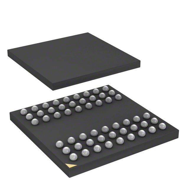
| Device Package | 54-TFBGA (8x8) | Memory Format | DRAM | Technology | SDRAM | ||
|---|---|---|---|---|---|---|---|
| Memory Size | 256 Mbit | Access Time | 5.4 ns | Grade | Industrial | ||
| Clock Frequency | 143 MHz | Voltage | 3V ~ 3.6V | Memory Type | Volatile | ||
| Operating Temperature | -40°C ~ 85°C (TA) | Write Cycle Time Word Page | N/A | Packaging | 54-TFBGA | ||
| Mounting Method | Volatile | Memory Interface | Parallel | Memory Organization | 16M x 16 | ||
| Moisture Sensitivity Level | 3 (168 Hours) | RoHS Compliance | ROHS Compliant | REACH Compliance | REACH Unaffected | ||
| Qualification | N/A | ECCN | EAR99 | HTS Code | 8542.32.0028 |
Overview of IS45S16160G-7BLA1 – 256Mbit SDRAM, 16M × 16, 54-TFBGA
The IS45S16160G-7BLA1 is a 256Mbit synchronous DRAM device from Integrated Silicon Solution Inc (ISSI) organized as 16M × 16 with a parallel memory interface. It implements a fully synchronous pipeline architecture and LVTTL-compatible signaling to support high-speed data transfer and burst-oriented memory access.
This device addresses designs requiring a 256Mbit parallel SDRAM with programmable burst length and sequence, selectable CAS latency, and on-chip refresh options, delivered in a compact 54-ball TFBGA package and operating over a -40°C to +85°C ambient range.
Key Features
- Memory Organization 256 Mbit capacity organized as 16M × 16 with internal bank architecture for row access/precharge management.
- Performance Speed grade -7 supports a clock frequency up to 143 MHz with an access time from clock of 5.4 ns and programmable CAS latency (2 or 3 clocks).
- Burst and Sequencing Programmable burst length (1, 2, 4, 8, full page) and selectable burst sequence (sequential or interleave) for flexible data transfer patterns.
- Refresh and Power Management Supports Auto Refresh and Self Refresh; refresh options include 8K refresh cycles every 32 ms (A2 grade) or 64 ms (commercial/industrial/A1 grade).
- Supply and Interface Single-supply operation at 3.0 V to 3.6 V (nominal 3.3 V ±0.3 V) with LVTTL-compatible inputs and a parallel memory interface.
- Package and Temperature Range 54-ball TFBGA (8 × 8) package; specified operating ambient temperature from -40°C to +85°C (TA).
Typical Applications
- Embedded Systems Use as high-performance parallel SDRAM in embedded platforms that require deterministic, synchronous memory access at up to 143 MHz.
- Buffer and Frame Memory Suited for data buffering or frame buffering where 16M × 16 organization and programmable burst transfers improve throughput.
- Industrial Electronics Applicable in industrial designs that need operation across a -40°C to +85°C ambient range and a 3.3 V single-supply memory solution.
Unique Advantages
- Deterministic synchronous operation Fully synchronous design with all signals referenced to the positive clock edge simplifies timing analysis and system integration.
- Flexible performance tuning Programmable CAS latency and burst options let designers balance latency, throughput, and access patterns for target workloads.
- Single 3.3 V supply Operates from 3.0 V to 3.6 V, minimizing the need for additional power rails and simplifying power supply design.
- Compact BGA package 54-ball TFBGA (8×8) reduces PCB area compared to larger packages while providing standard parallel SDRAM pinout.
- On-chip refresh management Auto Refresh and Self Refresh modes with supported refresh intervals reduce external controller overhead for memory retention.
Why Choose IC DRAM 256MBIT PAR 54TFBGA?
The IS45S16160G-7BLA1 positions itself as a straightforward, standards-based 256Mbit parallel SDRAM option for designs that require synchronous, burst-capable memory with configurable timing. Its 16M × 16 organization, programmable burst modes, and selectable CAS latency enable designers to adapt memory behavior to application-specific performance needs.
With single-supply 3.3 V operation, a compact 54-ball TFBGA footprint, and support for industrial ambient temperatures, this device is suitable for teams seeking a reliable memory building block from ISSI when deterministic synchronous DRAM behavior and on-chip refresh features are required.
Request a quote or submit a pricing inquiry to obtain part availability and lead-time information for the IS45S16160G-7BLA1.