IS45S16800E-7BLA1
| Part Description |
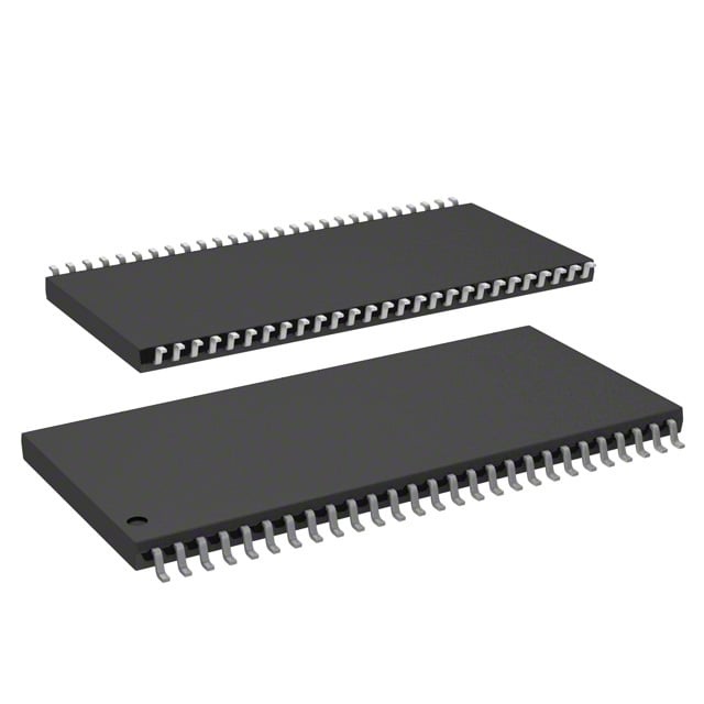
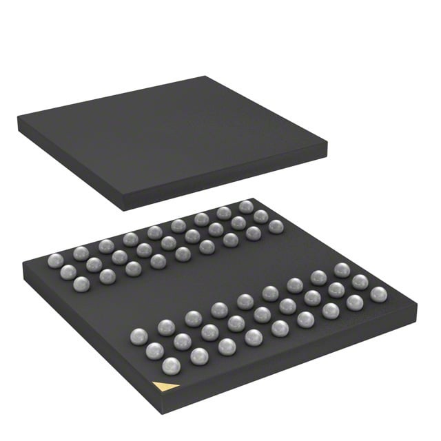
IC DRAM 128MBIT PAR 54TFBGA |
|---|---|
| Quantity | 1,246 Available (as of June 14, 2026) |
| Product Category | Memory |
|---|---|
| Manufacturer | Integrated Silicon Solution Inc |
| Manufacturing Status | Obsolete |
| Manufacturer Standard Lead Time | Contact Us |
| Datasheet |
Specifications & Environmental
| Device Package | 54-TFBGA (8x8) | Memory Format | DRAM | Technology | SDRAM | ||
|---|---|---|---|---|---|---|---|
| Memory Size | 128 Mbit | Access Time | 5.4 ns | Grade | Industrial | ||
| Clock Frequency | 143 MHz | Voltage | 3V ~ 3.6V | Memory Type | Volatile | ||
| Operating Temperature | -40°C ~ 85°C (TA) | Write Cycle Time Word Page | N/A | Packaging | 54-TFBGA | ||
| Mounting Method | Volatile | Memory Interface | Parallel | Memory Organization | 8M x 16 | ||
| Moisture Sensitivity Level | 3 (168 Hours) | RoHS Compliance | ROHS Compliant | REACH Compliance | REACH Unaffected | ||
| Qualification | N/A | ECCN | EAR99 | HTS Code | 8542.32.0002 |
Overview of IS45S16800E-7BLA1 – IC DRAM 128MBIT PAR 54TFBGA
The IS45S16800E-7BLA1 is a 128 Mbit synchronous DRAM (SDRAM) organized as 8M × 16 with a parallel LVTTL interface and a 54-ball TFBGA (8×8) package. The device implements a pipeline architecture and fully synchronous operation referenced to the rising edge of the clock, enabling high-speed, deterministic data transfer for memory buffering and burst-access applications.
Designed for 3.3 V memory systems, this part supports programmable burst lengths and CAS latency options, plus on-chip refresh and self-refresh functions for reliable dynamic memory operation across a wide operating temperature range.
Key Features
- Core / Architecture 128 Mbit SDRAM organized as 8M × 16 with quad-bank internal architecture and fully synchronous inputs/outputs referenced to clock rising edge.
- Memory Performance Clock frequency up to 143 MHz (‑7 speed grade); access time from clock 5.4 ns (CAS latency = 3). Programmable CAS latency of 2 or 3 clocks and random column address every clock cycle.
- Burst and Sequencing Programmable burst length (1, 2, 4, 8, full page) and selectable burst sequence (sequential or interleave) with burst read/write capability and burst termination support.
- Refresh and Power Modes Auto Refresh and Self Refresh supported. Refresh options include 4096 cycles every 16 ms (A2 grade) or every 64 ms (A1 grade) as specified in the device datasheet.
- Interface LVTTL-compatible parallel interface for synchronous system integration.
- Power Supply Specified for 3.3 V VDD and VDDQ (device designed for 3.3 V memory systems); acceptable supply range indicated in product specifications.
- Package & Temperature 54-ball TFBGA (8×8) package; operating temperature range listed as −40 °C to +85 °C (TA) for the A1 option in the product specifications.
Typical Applications
- High‑speed data buffering Use as frame buffers or transient data buffers where synchronous, burst-capable memory is required for fast read/write bursts.
- System memory for embedded platforms Provides deterministic, clock-referenced storage for embedded designs requiring parallel SDRAM with programmable CAS latency.
- Signal processing and buffering Suitable for applications that benefit from pipeline architecture and random column access every clock cycle for streaming data operations.
Unique Advantages
- Deterministic synchronous operation: Fully synchronous inputs/outputs referenced to clock edges simplify timing and integration in clocked systems.
- Flexible performance tuning: Programmable CAS latency and burst length/sequence let designers balance latency, throughput, and bus utilization.
- On‑chip refresh management: Auto Refresh and Self Refresh reduce external refresh overhead and support power-saving modes in system designs.
- Compact BGA footprint: 54-ball TFBGA (8×8) package offers a small form factor for space-constrained board layouts.
- Wide operating range: Device data supports operation down to −40 °C, enabling deployment across a broad temperature envelope defined in the datasheet.
Why Choose IC DRAM 128MBIT PAR 54TFBGA?
The IS45S16800E-7BLA1 delivers synchronous, burst-capable 128 Mbit memory with programmable timing and refresh features that make it suitable for designs requiring predictable high-speed parallel memory. Its 8M × 16 organization, LVTTL interface, and 54-ball TFBGA package provide a balance of density and board-level integration for embedded platforms and buffering applications.
This SDRAM is positioned for engineers seeking a 3.3 V synchronous DRAM solution with configurable latency and burst behavior, on-chip refresh capabilities, and a compact package. The device specification and timing options support scalable designs where system-level timing control and deterministic memory access are important.
Request a quote or submit an inquiry to obtain pricing and availability for IS45S16800E-7BLA1 and to discuss quantity-based lead times or technical integration support.